Datanami
 EnterpriseAI
 HPCwire Japan
 QCwire
 HPC & AI Wall Street
Here is a collection of highlights from this week’s news stream as reported by HPCwire.
German GPU-CPU Supercomputer Managed with Bright Cluster Manager
T-Platforms to Build Russia’s First Petaflops Supercomputer
HyperTransport Consortium Unveils HyperShare Platform
CERN Selects Brocade to Bolster Network Performance and Support Growth Plans
Scientists Ratchet Up Understanding of Cellular Protein Factory
Jaguar Pounces on Child Predators
Argonne Selects Allinea Software to Improve Debugging Performance Scalability on Blue Gene/P
RenderStream Announces 12 Teraflop Systems
Siemens Intends to Intensify the Development of Industrial Software
Mellanox to Acquire Voltaire for $218 Million
Blue Waters Staff, Partners Bring Home Awards from SC10
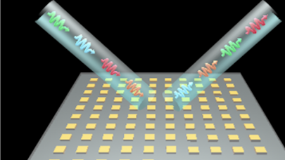
Short, On-Chip Light Pulses Will Enable Ultrafast Data Transfer Within Computers
Cancer Research UK, Imperial College London Celebrate HPC Supercomputing Successes
Startup Dezineforce Launches ‘Black Box’ Technical Computing Server
2010 INCITE Awards Announced
The 2010 “INCITE” Program awards were announced this week, and they’re the largest yet — nearly 1.7 billion processor hours on the Department of Energy’s world-class supercomputers will be shared among 57 research projects. This year’s INCITE program brings us a step closer to scientific breakthroughs in biofuels, nuclear power, medicine and climate change. To help explain the significance of the award to the non-technical among us, the announcement cited a combined computing power equal to 135,000 quad-core laptops. The 57 winning applicants will be able to perform simulations and virtual experiments that would otherwise be impractical in the “real” world.
U.S. Energy Secretary Steven Chu, who announced the awards, made the following statement: “The Department of Energy’s supercomputers provide an enormous competitive advantage for the United States. This is a great example of how investments in innovation can help lead the way to new industries, new jobs, and new opportunities for America to succeed in the global marketplace.”
The projects include both academic and commercial endeavors. Partnerships with companies such as GE and Boeing are in place that use advanced computer modeling for the development of better wind turbines and jet engines. Other projects will work toward designing more efficient solar cells, developing fusion energy systems, and increasing the effectiveness of medications for slowing the progression of Parkinson’s disease.
The Innovative and Novel Computational Impact on Theory and Experiment (INCITE) program is the U.S. government’s premier supercomputing allocation. It is open to all scientists and projects are selected competitively based on their potential to advance scientific discovery. INCITE is supported by the DOE’s Office of Science and managed by the DOE Leadership Computing Facilities at the Department’s Argonne and Oak Ridge National Laboratories.
The Oak Ridge Leadership Computing Facility (OLCF) at Oak Ridge National Laboratory has been awarded 950 million processor hours and will host thirty projects with the power of the Jaguar supercomputer, a Cray XT5 capable of 2.33 petaflops of peak performance power.
Four projects from Argonne National Laboratory have been awarded a total of 65 million hours of computing time on Argonne’s Blue Gene/P (“Intrepid”) supercomputer. As well, Argonne scientists will participate in six other projects (led by other instutions).
Going back to the laptop comparison, Jaguar has a computational capacity of approximately 109,000 laptops, and Intrepid is roughly equivalent to 26,000 laptops.
OLCF Director of Science Bronson Messer, remarked on the high quality of the submissions: “This year’s group of proposals was probably the best we’ve seen to date. The final list of awardees is a collection of projects that we believe will have remarkably high scientific impact through the use of leadership computing resources.”
A detailed listing of awards is available here (PDF).
Optical Chip Technology from IBM Could Be Key Exascale Enabler
IBM researchers have announced a breakthrough that allows computer chips to communicate using pulses of light instead of electrical signals. The new technology — called CMOS Integrated Silicon Nanophotonics — integrates electrical and optical devices on the same piece of silicon, resulting in smaller, faster and more power-efficient processors.
Nanoscale silicon photonics offers immense technical advantages over current copper interconnect technologies and promises to meet the increasing bandwidth demands of high-performance computing systems. Indeed, this latest advance could hold the key to exascale computing – supercomputers that are one thousand times faster than today’s petasflop-level machines.
This breakthrough comes after a decade of development at IBM’s global Research laboratories and signals a new era in chip communication. Placing optical devices and functions directly onto a silicon chip offers more than 10X improvement in integration density over current technologies. What’s more, the new chips can be manufactured in a standard CMOS foundry and do not require any special tools, making it cost-effective.
Dr. T.C. Chen, vice president of Science and Technology at IBM Research, reports:
“The development of the Silicon Nanophotonics technology brings the vision of on-chip optical interconnections much closer to reality. With optical communications embedded into the processor chips, the prospect of building power-efficient computer systems with performance at the exaflop level is one step closer to reality.”
In an article at PCWorld, Will Green, a silicon photonics research scientist at IBM, reported that this latest breakthrough puts IBM on course to building an exascale computer by 2020.
Dr. Yurii A. Vlasov, manager of the Silicon Nanophotonics Department at IBM Research, offers more details:
“Our CMOS Integrated Nanophotonics breakthrough promises unprecedented increases in silicon chip function and performance via ubiquitous low-power optical communications between racks, modules, chips or even within a single chip itself. The next step in this advancement is to establishing manufacturability of this process in a commercial foundry using IBM deeply scaled CMOS processes.”
IBM’s stated goal is to integrate ultra-compact nanophotonic circuits onto the die to allow for the manipulation of light signals similar to the way electrical signals are manipulated in computer chips. The end game here is the creation of a 3D-integrated chip, a viable next-generation chip technology that promises to postpone the much-prophesized death of Moore’s Law.