Datanami
 EnterpriseAI
 HPCwire Japan
 QCwire
 HPC & AI Wall Street
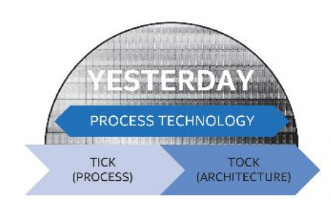
In a recent 10-K filing (an annual report to the US Securities and Exchange commission), Intel announced that it is retiring its 24-month tick-tock development model and replacing it with a 30-month ‘process, architecture, optimization’ model.
“We expect to lengthen the amount of time we will utilize our 14nm and our next generation 10nm process technologies, further optimizing our products and process technologies while meeting the yearly market cadence for product introductions,” Intel said. The comment was supported by a graphical depiction of the change (below).

For nearly a decade, Intel has followed a tick-tock innovation cycle — “tick” being a shrinking of process technology with “tock” being a new microarchitecture. The 24-month deployment schedule was notable for adhering to Moore’s law, the legacy of Intel’s Gordon E. Moore, who in 1965 anticipated that transistor density would double roughly every two years.
The announcement marks a formal acknowledgement of a stretched-out design schedule, but the tick-tock cadence had already been slipping. The Haswell Refresh (mid-2014) was the first sign of syncopation and when, in July 2015, Intel inserted Kaby Lake into its roadmap, it was clear that the Haswell Refresh semi-tock hadn’t been an anomaly. Originally, the 10nm Cannonlake was to succeed the 14nm Skylake microarchitecture, but with the insertion of the 14nm Kaby Lake, the 10nm node change is being postponed until the second half of 2017.
Despite continued assertions from Intel that Moore’s law is alive and well, the new development cycle speaks to the difficulties of innovating at smaller and smaller node sizes.
The worldwide semiconductor industry is not only acknowledging that Moore’s law is in trouble, it is actively preparing for its demise. Details of the Semiconductor Industry Association’s forthcoming technology roadmap were expounded on in the journal Nature.
Author of the Nature article M. Mitchell Waldrop writes:
…The doubling has already started to falter, thanks to the heat that is unavoidably generated when more and more silicon circuitry is jammed into the same small area. And some even more fundamental limits loom less than a decade away. Top-of-the-line microprocessors currently have circuit features that are around 14 nanometres across, smaller than most viruses. But by the early 2020s, says Paolo Gargini, chair of the road-mapping organization, “even with super-aggressive efforts, we’ll get to the 2–3-nanometre limit, where features are just 10 atoms across. Is that a device at all?” Probably not — if only because at that scale, electron behaviour will be governed by quantum uncertainties that will make transistors hopelessly unreliable. And despite vigorous research efforts, there is no obvious successor to today’s silicon technology.
Because of this, the SIA roadmap is beginning to pivot away from Moore’s law:
The industry road map released next month will for the first time lay out a research and development plan that is not centred on Moore’s law. Instead, it will follow what might be called the More than Moore strategy: rather than making the chips better and letting the applications follow, it will start with applications — from smartphones and supercomputers to data centres in the cloud — and work downwards to see what chips are needed to support them. Among those chips will be new generations of sensors, power-management circuits and other silicon devices required by a world in which computing is increasingly mobile.
Intel remains unfazed by the public perception around Moore’s law. Their message to the community has been that there is a virtuous cycle between supercomputing and chip design and that while there are natural ebbs and flows, Moore’s law is as strong as ever.
“While some naysayers in the industry have sounded the death knell for Moore’s Law—as they have since time immemorial—it is Intel’s business to continue it,” wrote Intel’s Mark Stettler and Shesha Krishnapura in an article for HPCwire earlier this year. “It’s an unwritten law in engineering that every generation thinks their challenges are the most difficult. Although new technical challenges continue to emerge, as they have every generation since the first VLSI chips were created, the outlook for Moore’s Law remains the same as it did twenty years ago; the path for the next few generations is visible, and after that, it gets hazy until we move forward.”