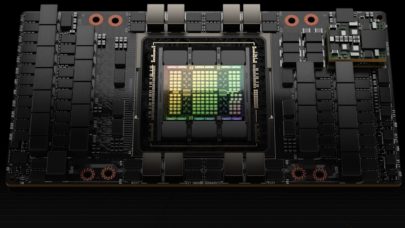
With Intel’s manycore MIC coprocessor looming on the horizon, NVIDIA’s is counting on its upcoming K20 Tesla to retain its dominance in the HPC accelerator marketplace. And while Intel has shared few technical details about its upcoming Knights Corner MIC, NVIDIA has conveniently provided a 24-page white paper (PDF) describing the inner workings of the GK110, the GPU that will power the K20 card for supercomputers.
If you’re a GPU programmer and like to get intimate with the silicon, or are just curious about where NVIDIA is heading with GPU computing, the GK110 paper should be on your summer reading list. It contains a nice description of the GK110 architecture and goes into some depth on the new features that this high-end Kepler brings to the HPC table.

As we described in our Kepler launch coverage last week at the GPU Technology Conference, the big new features in the architecture are Hyper-Q and Dynamic Parallelism. Both are changes that aim to relieve the CPU-GPU bottleneck, enabling the GPU to be better utilized for continuous processing, and freeing up the CPU for more mundane serial tasks. Those two features, however, are only available in the supercomputing-grade GK110, not the GK104 that powers the less powerful K10 card.
To recap, Hyper-Q allows the GPU to execute up to 32 MPI processes, CUDA streams, or threads at the same time. The Fermi GPU could only manage a single task at a time, which limited how much true parallelism the application could attain, and, in many cases, how much of the GPU could be utilized at any particular moment. Hyper-Q should automagically speed up a lot of existing CUDA applications without the need for any source code changes.
Dynamic parallelism, on the other hand, will require some source tweaking for existing GPU code, since it enables programmers to explicitly place more of the application on the graphics chip. It basically allows the GPU to generate work on its own, without having to rely on the CPU to keep feeding it. With dynamic parallelism, a kernel can now launch another kernel, enabling recursive and nested execution. For codes not yet ported to GPUs, this is good news, since this style of programming is a much more natural way to write applications.
Along those same lines is GPUDirect, a hardware/software-enabled feature that allows GPUs to talk to one another directly as peers, bypassing the CPU entirely. GPUDirect was present in Fermi, but the new Kepler has additional support that further lessens its reliance on the CPU. Using this feature, a GPU would be able to go through the NIC and exchange data with other GPUs on the network without CPU buffering in main memory. It also enables other PCIe attached devices, like SSDs, to directly access GPU data.
The NVIDIA engineers have also included some other tweaks to support greater application complexity. One of these is quadrupling the register count per thread compared to the Fermi architecture (from 63 to 255). Routines that do a lot of register spilling to memory because they have to deal with so many variables, like those in quantum chromodynamics, could see some pretty significant speed-ups, according to NVIDIA.
The GK110 also adds an extra 48K read-only data cache per multiprocessor for local functions. The new GPU also doubles the L2 cache capacity, to 1,536 KB, which helps data-dependent codes like physics solvers, ray tracing, and sparse matrix multiplication. This is all in addition to the 64 KB of multiprocessor memory (to divide between L1 and shared data) that Kepler inherited from Fermi, but which now supports more bandwidth for large reads.
All of this is geared to boost application performance in a big way. Here though, the paper hedges on the specifics, promising only “over 1 teraflop of double precision throughput.” NVIDIA is claiming the Kepler will deliver three times the performance per watt of the Fermi GPUs, but that doesn’t necessarily map to peak performance on a given chip. With regard to that metric, we should probably except a doubling or so of the Fermi Tesla’s 665 gigaflops for the top-of-the line Kepler hardware.
But application performance with the GK100 is expected to do much better that with the Fermi-generation GPUs. To a large degree that’s due to all the aforementioned CPU-offload features and other architectural tweaks. But a good chunk of the performance boost will be delivered via brute force, in the form of lots of cores.
The paper says the “full” GK110 implementation will have 15 streaming multiprocessor (SMX units), each of which has 192 cores. That would make the top Kepler a 2,880-core processor, which beats out the 512-core Fermi by a wide margin. But all those cores will be running at about half the clock speed as its predecessor. As the GK110 white paper explains:
For Kepler, our priority was performance per watt. While we made many optimizations that benefitted both area and power, we chose to optimize for power even at the expense of some added area cost, with a larger number of processing cores running at the lower, less power-hungry GPU clock.
The increased core count is enabled by a transistor shrink, in this case, TSMC’s 28nm process technology. In fact, the GK110 will be the largest processor ever built, at least the largest one that is not still sitting in a research lab somewhere. At 7.1 billion transistors, the GK110 is nearly twice the size of the new 4.3 billion transistor Radeon HD 7900 GPU from AMD. For some context, the new “Sandy Bridge” Xeon E5-2600 series CPUs are made up of less than 2.3 billion transistors.
There will also be two slightly smaller GK110 GPU parts, with 13 and 14 multiprocessors, respectively. Presumably the clock frequencies could be cranked up a bit on those if faster thread performance is desired, or down if lower wattage is the goal. In any case, the three GK110 variants suggests NVIDIA will offer a range of HPC products aimed at different price/performance/power points.
The first GK110 GPUs are expected to debut in the K20 Tesla cards in Q4. NVIDIA might be initially hard-pressed to ramp up volumes, especially since TSMC has a number of customers (AMD and Qualcomm, in particular) also vying for 28nm capacity. Supposedly though, NVIDIA chips are going to be priority at the foundry. Even so, such a big chip might still be a challenge for TSMC, from a yield perspective.
In any case, most, if not all of the early GK110s will likely end up in just two systems: the DOE’s Titan supercomputer at Oak Ridge National Lab and the NSF’s Blue Waters machine at NCSA. About 15,000 of the GK100s are expected to go into the Titan super, while the more conservative Blue Waters system will be equipped with around 3,000 of new GPUs.
NVIDIA expects to sell a lot more of them that over the next two or three years, until the “Maxwell” GPU kicks in. That architecture is expected to encompass CPU-GPU integration, the so-called “Project Denver” work that glues a 64-bit ARM CPU onto a CUDA GPU. As such, it will represent an architectural watershed for NVIDIA, but one that Kepler laid the groundwork for.
Kepler, and the GK110 in particular, is NVIDIA’s most general-purpose processor to date. By reducing the dependency of the GPU on the CPU, and making the GPU more capable of supporting complex types of processing, NVIDIA is not just trying to make the two architectures equal peers, but to make the GPU the star of the show. If NVIDIA continues to pursue this architectural trend line, the CPU, while necessary, could be reduced to the role of an OS microcontroller: fielding interrupts, managing I/O, and scheduling jobs. The GPU, meanwhile, would be able to encompass the high-value application processing, which not only conforms to NVIDIA’s philosophical bent, but also its business strategy.


