Datanami
 EnterpriseAI
 HPCwire Japan
 QCwire
 HPC & AI Wall Street
Intel has finally pulled the lid off their Westmere-followup processors with the new Xeon E7 v2 series, which while generally targeting enterprise big data and analytics workloads, offers far more for HPC than might meet the eye.
Despite the range of targeted application areas, the 22 nanometer process, memory capabilities, robust AVX instruction capabilities, and unique reliability features make this well suited for HPC. Intel has managed to slice a sizable piece of performance to create a 120-core “HPC cluster in a box” that while higher in price than the previous Ivy Bridges that rolled out last September, could be a suitable fit for a wide swath of technical computing workloads.
As Intel’s Joe Curley told us today, “The E7s offer a ton of density in a node and this is indeed a great HPC story–as well as a great big data and enterprise story. Any type of application where you need a lot of memory and reliability and you’re doing a long set of calculations, that’s where the E7 set of products is going to do really well for you.” You end up with 120 cores in a node, 12 terabytes of memory maximum, you can fit a lot of density and compute there and there are HPC and many other workloads that this will be ideal for.”
Before we dive into the specifics, it’s worth acknowledging that one of the most fascinating aspects of this more general E7 v2 announcement is how Intel was able to balance out a multitude of goals and targets for a wide range of potential workloads via a segmentation model. It would have been perfectly feasible for this same news to span across several versions of the same essential chip sporting variations in cache or clock speeds—but these are actually well-optimized for the workloads being targeted and can be broken down along multiple lines according to priorities (power draw, memory and cache requirements, clock speed, etc.). In other words, the marketing for the E7 v2 is that there’s almost guaranteed to be something for everyone, in all price ranges and across nearly all workloads.
For context, take a look below at the two comparison charts that compare the Westmere predecessor (the E7-4800) with against SPEC (at the top) and then according to LINPACK performance just underneath.
 And for LINPACK

The AVX capabilities are another noteworthy feature in these new processors—a point to consider with the LINPACK slide above. The 256-bit AVX vector units in the Ivy Bridge core can do eight double-precision floating point calculations per clock cycle via two AVX units per core (4 per AVX unit). This is good news for HPC on this front since the Westmere didn’t have any AVX at all.
The thing to notice here is that if you look below at the figures with 15 cores operating on this level, you’re looking at 1.246 teraflops—which is right on par with the Xeon Phi. Theoretically, this means that for those who aren’t concerned with the price (and the difference is quite hefty) it’s possible to circumvent the Xeon Phi and the programming talent required to get code up to snuff entirely and stock a cluster with these parts instead. Whether or not shops will consider this is up in the air—especially since this comparison won’t be valid by next year if rumors are correct and a three-teraflop Phi chip actually emerges.
According to Curley, “The products complement each other. Each Xeon Phi coprocessor has greater peak FLOPS and memory bandwidth per device, but lower memory capacity. The Xeon E7 Family provides very large memory capacity per processor, and allows up to 8 processors per node.”
The products address different application spaces for the most part, but as part of a portfolio produce an outstanding economic return for application developers, said Curley. “The Intel Xeon E7 Family is optimized for computing with memory density per node, superior results when compared to RISC and mainframe alternatives, and server consolidation markets. Xeon Phi addresses highly parallel applications that can take maximum benefit of Xeon Phi’s performance per watt.”
But the key advantage between them remains that applications optimized for Xeon Phi use the same core, thread, and SIMD elements – meaning applications optimized for one can be moved to the other – a critical advantage for developers.
Take a look at the chart below, which shows the 20 ways you can slice the E7 v2 for 2, 4 and 8 socket variants across different workload types via the basic, standard and advanced configurations, all of which offer some notable tradeoffs (or none at all for the big spenders) in core counts, cache and clock speeds to fit a variety of both memory, compute and energy demands. The segment optimized for HPC (bottom right with my red arrow) the E7 8857 v2, is available in an 8-socket version only with 12 cores running at 3.0 GHz in 30 megabytes of cache in 130 watt envelope for $3838 (versus the other 8-socket optimized variants that offer 3.2 ghz clockspeed, full cache and of course, more cores. The fact that specific optimized part is only available in 8-socket is definitely noteworthy; Intel has always offered 2 and 4-socket versions of previous offerings.
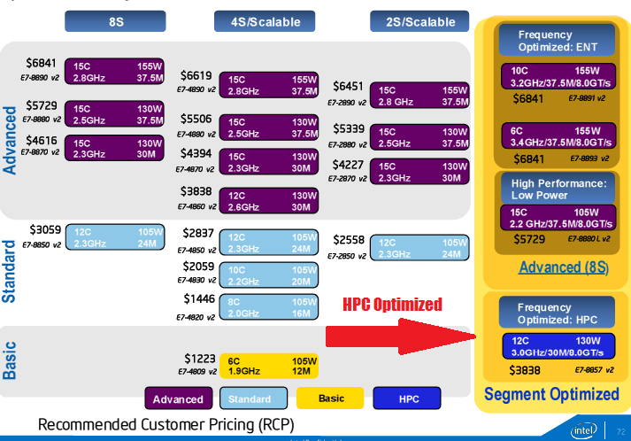
Intel’s Curley told us that while there is a segment optimized offering in 8-node configuration, this by no means limits the options for HPC shops and OEMs. “If you wanted to try to build big a lot of memory capacity or bandwidth on a two-socket node you could use smaller E7 line products. OEMs will configure this in a number of ways. There are different feature sets across the line; the line is built for the greatest memory density per core, it has a lot of bandwidth per core, it’s built for even greater levels of resiliency to support mission-critical applications in ways that previous generations didn’t address to this degree.” In other words, as with everything in HPC–it all depends on where your priorities lie.
In this E7 world of multiple possibilities, there are a number of configurations that serve different needs, as highlighted below. As Intel demonstrates via the 120-core cluster in a box-themed slide below, if you have four 2-socket servers of the previous generation, you can do the same amount of work by jamming it into two four-socket servers, but run at around 2.5x faster (thanks to the QuickPath Interconnect, which is way faster than Ethernet).
 The beauty of the model is that for HPC workloads in particular (keep in mind that the sweet spot for average job sizes in HPC hovers around the 128 core mark) it’s possible to speed up the work using the same number of processors and farm it out to larger, more memory-stuffed nodes that are designed to run faster.
To put this in some real-world performance context, consider the (somewhat wonky) chart below, which uses the baseline of the Ivy Bridge they rolled out last September. Intel wasn’t crossing out their own numbers there; rather, the crossed-out number represents the average performance boost for a broad range of similar workloads—in essence, an average figure across multiple applications in a domain. The higher number with the application name is a top performer, hitting the app high-water mark they reference on the top left.
In other words, using the life sciences example, while most life science applications they benchmarked came out at around 2x the performance, MILC hit 3x. Similarly, when it came to financial services, the average performance increase across a range of common applications was 2.4 while Black Scholes in particular topped out at 2.6x. Even without data on how many applications were benchmarked to come up with the average, you get the idea…
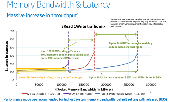
 On another note, for those who are interested in bandwidth, Intel has had single device data correct, or SDDC, in the memory controllers used with its server processors since the 1990s. What it does, in essence anyway, is allow for a faulty DRAM memory chip to be taken out of the memory pool and isolated. You can heal around one bad chip and correct errors. With the Westmere E7s, given the large memory in the system, Intel added a new feature called Double Device Data Correct.
With this feature, Intel could correct errors after two chips failed on a memory module. With the new performance mode, Intel is allowing customers who want to speed up the memory buffer chips and therefore get more memory bandwidth out of the system to step back to single chip recovery mode. In the normal DDDC mode, which is called lockstep mode now, both the SMI2 memory buffers and the memory chips run at the same speed: 1600 MT/sec. With the new performance mode, the SMI2 memory buffers run at 2667 MT/sec, and the memory runs at half that speed. The net effect is that in performance mode, the system bandwidth is increased by 54 percent compared to lockstep mode. Some error correction capability is sacrificed for the sake of bandwidth.
All of this theoretical at this point, mind you–we can write the real story when some early users lend us their experiences and insights. As it stands, this story just broke and again, the real emphasis is on databases (the SAP HANA tale is certainly compelling–follow that at EnterpriseTech this week).