Datanami
 EnterpriseAI
 HPCwire Japan
 QCwire
 HPC & AI Wall Street
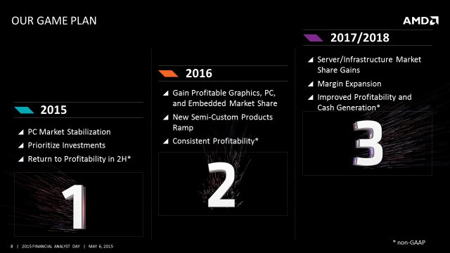
AMD revealed key elements of its multi-year strategy as part of its 2015 Financial Analyst Day event in New York on Wednesday. Out of the gate, CEO Lisa Su acknowledged the company’s recent challenges, pointing to a weak PC market and market share losses, before turning her attention to the game plan that AMD is counting on to turn its earnings statement from red to green. It’s a game plan that has AMD returning to the high-end server space as it seeks to diversify its revenue base and grow into new markets.
“We are focused on areas that require high performance compute, high performance graphics, visualization technologies, and complex system on chips,” said Su, who kicked off the proceedings, “those are the areas that are uniquely suited to AMD…and we think this represents about a $60+ billion TAM.”
“Datacenter is probably the single biggest bet that we are making as a company,” she declared. “We have not been competitive the last few years, we will be competitive in the datacenter market.”
Su also spoke about the decision to exit the SeaMicro dense server system business line “for one because microservers were not growing as fast as originally thought and two we really aren’t a systems company, however on the silicon side, very very clearly we are an x86 company, we have tremendous x86 heritage and are absolutely going to invest in high-performance x86.”
With regard to technology, Su said that AMD portfolio decisions will be focused on high-performance cores, immersive technologies, 2.5/3D packaging and software/APIs. This will align with increased x86 investment, focused ARM investment and a simplified CPU roadmap.
Su also offered an appeasement for those wondering why AMD didn’t make these changes sooner.
“On the platform side, to those of you that ask what have you guys been doing for a couple of years. The truth is, it takes a while to really transform both the R&D capabilities, the technologies and the modularity,” she said.
And now…Getting Zen with simplified roadmaps
The highlight of AMD’s revamped technology roadmap is a brand new x86 processor core codenamed “Zen,” touting improved instructions per clock of up to 40 percent over “Excavator” cores. Absent from the lineup, however, is the Skybridge project. Announced last year, the plan to join x86 and ARM together on a common platform was dropped, according to Su, due to customer feedback indicating a desire for x86 and ARM, but not necessarily in socket-compatible factors.

Mark Papermaster, AMD chief technology officer and senior vice president, addressed AMD’s x86 positioning and laid out some of Zen’s specs in anticipation of its 2016 debut. AMD is counting on its new Zen core to drive its re-entry into high-performance desktop and server markets and put it back on a competitive track against arch rival Intel.
“It’s got high-throughput, very efficient design, and a new cache and memory subsystem design to feed this core,” he said, referring to the feature of simultaneous multi-threading (SMT). The performance is the result of doubling down on the previous generation core, Excavator, due out this summer, said Papermaster.
“This wasn’t one silver bullet,” Papermaster continued, “but a number of elements combining to drive the microarchitecture improvement and deliver what I’ve not seen in the industry before, a 40 percent improvement in instructions per clock.”
It’s the core design for the workload of the future and it’s available next year, he added. It’s also a commitment to sustainable innovation, according to Papermaster, who says the company has leapfrogging design teams and is already working on the successor to Zen as it works to establish a family of cores over time.
Papermaster also revealed that AMD’s first custom 64-bit ARM core, “K12” core, is on track for a 2017 sampling. These enterprise-class ARM cores are designed for efficiency and are intended for server and embedded workloads.

On the graphics side, AMD is readying to launch its high-performance graphics processing unit (GPU) with die stacked High Bandwidth Memory (HBM) using a 2.5D silicon interposer design. This core is optimized for graphics and parallel compute and includes a number of other enhancements (depicted in the slide below). AMD reported that future generations of its high-performance GPUs will be based on FinFET process technology, which will contribute to a doubling of performance-per-watt.

These three essential chip technologies will be the building blocks of AMD’s Enterprise, Embedded and Semi-Custom Business Group (EESC). A new group launched in 2014 as part of AMD’s business unit reorganization, EESC is focused on high-priority markets that will leverage high-performance CPU and GPU cores inside differentiated solutions.
Forrest Norrod, senior vice president and general manager of the business group, referred to the EESC segment as “a principal driver of growth for the last few years and one we think is central to the growth story of AMD going forward.”
Norrod added that these three businesses (enterprise, embedded and semi-custom) share a perspective around the best way to showcase AMD technology.
“In all of these businesses our customers are building products around the technology ingredients that we give to them and bringing differentiated solutions to the end customer that leverage AMD unique IP,” he stated.
“So we really think now of ESSC as being a continuum leveraging technology, customer relationships and the modular design approach at both the chip as well as the systems level.”
Norad went on to share in broad strokes AMD’s datacenter roadmap for the 2016-2017 timeframe, which includes its next-gen x86 Opteron, next-gen ARM, and an APU that we will be tracking closely.

The upcoming next-generation AMD Opteron processors are based on the x86 “Zen” core and target mainstream servers. These x86 Opterons tout high core count with full multi-threading, disruptive memory bandwidth and high native I/O capacity. Norrrod also introduced “the highest performance ARM server GPUs,” powered by AMD’s upcoming “K12” core.
Most relevant for HPC, though, is the new high-performance server APU, a multi-teraflops chip targeting HPC and workstation markets.
“We’re bringing the APU concept fully into the server realm,” Norrod stated. “These are high performance server APUs offering not just high-performance CPU cores and memory but multi-teraflops GPU-capability, providing a level of performance for machine learning, a level of performance for finite element analysis, and a level of performance for memory bandwidth for reverse time migration algorithms that the oil companies use to do reservoir simulation.”
The APU line (APU stands for accelerated processing unit) is an outcome of the Fusion project, which started in 2006 with AMD’s acquisition of the graphics chipset manufacturer ATI. AMD has talked up the potential benefits of tight CPU-GPU integration for HPC workloads in the past, but until now AMD’s APU efforts have primarily been relegated to desktop space.
In January 2012, AMD rebranded the Fusion platform as the Heterogeneous Systems Architecture (HSA) and has in recent months begun championing the CPU+accelerator architecture for a wide range of workloads, including HPC.
AMD says the next-gen server APU stands to deliver massive improvements to vector applications with scale-up graphics performance, HSA enablement, and optimized memory architecture. “We think we’ve got unique and compelling technology that is only possible by wedding together the CPU and world-class GPU and combining them with an open standard HSA software interface,” said Norrod.
What’s not clear at this point is whether the APU’s multi-teraflops will be of the half- single- or double-precision variety, and the workloads that Norrod lists are a mixed bag in that respect (FEA and machine learning, for example). Of course, there is no reason AMD can’t launch variants for each, but it would be hard to claim HPC cred without an FP64-heavy version.