 Datanami
 EnterpriseAI
 HPCwire Japan
 QCwire
 HPC & AI Wall Street
Combining electronics and photonics on semiconductor microchips to speed data transmission isn’t a new idea – the potential for better performance and power reduction are enticing. However thorny manufacturing issues have so far limited widespread use of this approach. That could change soon according to a recent report in Nature[i] and would have have broad implications extending even to efforts to achieve exascale computing, say the authors.
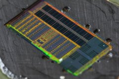
In the paper – “Single-chip microprocessor that communicates directly using light” – researchers from UC Berkeley, University of Colorado, and MIT report fabricating an electronic–photonic system on a single chip integrating over 70 million transistors and 850 photonic components that work together to provide logic, memory, and interconnect functions. Most significantly, they did it with standard CMOS manufacturing techniques.
Talking about the impact of the work, Miloš Popovic a co-author on the study from the University of Colorado told HPCwire, “This work is directly aimed at the energy problem in supercomputers. It will enable reducing the communication energy by about an order of magnitude, and will make communication energy independent of distance of a link — up to 100’s of meters. So, it’s definitely part of the exascale computing story.”
The chip was fabricated using a commercial high-performance 45-nm complementary metal–oxide semiconductor (CMOS) silicon-on-insulator (SOI) process. The authors write: “No changes to the foundry process were necessary to accommodate photonics and all optical devices were designed to comply with the native process-manufacturing rules. This ‘zero-change’ integration enables high-performance transistors on the same chip as optics, reuse of all existing designs in the process, compatibility with electronics design tools, and manufacturing in an existing high-volume foundry.”
On-chip electro-optic transmitters and receivers enable both the microprocessor and the memory to communicate directly to off-chip components using light, without the need for separate chips or components to host the optical devices.
One advantage of light based communication, noted Popović, is that multiple parallel data streams encoded on different colors of light can be sent over one and the same medium – in this case, an optical wire waveguide on a chip, or an off-chip optical fiber of the same kind that as those that form the Internet backbone.
“Another advantage is that the infrared light that we use – and that also TV remotes use – has a physical wavelength shorter than 1 micron, about one hundredth of the thickness of a human hair,” he said. “This enables very dense packing of light communication ports on a chip, enabling huge total bandwidth.” The new chip has a bandwidth density of 300 gigabits per second per square millimeter, about 10 to 50 times greater than packaged electrical-only microprocessors currently on the market.
The big news is the relative ease of manufacture. “This “zero change” approach to integration enables complex electronic-photonic systems on chip to be designed today, in an advanced CMOS foundry. This means high yield, immediate transition to volume production, and the most advanced transistors of any photonic chip (and the largest number of them). These qualities should open up research into systems on chip in many applications including RF signal processing, radar/lidar applications, sensing and imaging, etc.
The authors note, “By showing that a microprocessor with photonic I/O is possible to build today, we’re illustrating the power of this approach. Incidentally, while we expected photonic devices to not perform as well using this approach as using fabrication customized to photonics, it turns out that in a number of cases they perform better — leveraging the high resolution implant masks, controlled sub-100nm CMOS deep UV lithography, and rich set of material and mask levels available in CMOS.”
As described in the paper, the manufacturing process includes a crystalline-silicon layer that is patterned to form both the body of the electronic transistors and the core of the optical waveguides. A thin buried-oxide layer separates the crystalline-silicon layer from the silicon-handle wafer. Because the buried-oxide layer is <200 nm thick, light propagating in crystalline-silicon waveguides will evanescently leak into the silicon-handle wafer, resulting in high waveguide loss.
To control leakage, selective substrate removal was performed on the chips after electrical packaging to etch away the silicon handle under regions with optical devices. The silicon handle remains intact under the microprocessor and memory (which dissipate the most power) to allow a heat sink to be contacted, if necessary. The researchers report removal of substrate “has a negligible effect on the electronics and the processor is completely functional even with a fully removed substrate.” The full details are best gleaned from the paper itself.
Researchers built the photodetectors of Silicon-Germanium (SiGe), which is present in small amounts in advanced CMOS processing, and selected 1,180nm wavelength for the optical channels as silicon is transparent to that wavelength. No adverse effects were seen and propagation losses were 4.3 dB/cm. The electro-optic transmitter consists of an electro-optic modulator and its electronic driver. The modulator is a silicon micro-ring resonator with a diameter of 10 μm, coupled to a waveguide.
It was necessary to create a tuning mechanism report the authors: “As a resonant device, the modulator is highly sensitive to variations in the thickness of the crystalline-silicon layer within and across SOI wafers as well as to spatially and rapidly temporally varying thermal environments created by the electrical components on the chip. Both effects cause λ0 to deviate from the design value, necessitating tuning circuitry. We embedded a 400-Ω resistive microheater inside the ring to efficiently tune λ0 and added a monitoring photodetector weakly coupled to the modulator drop port. When light resonates in the modulator ring, a small fraction of it couples to and illuminates the photodetector.”
Sadasivan Shankar, a longtime senior Intel researcher in semiconductor manufacturing and currently a visiting lecturer in computational science and engineering at Harvard, called the work important. “As mentioned in the paper itself, this is the current strained transistor technology that has been available in the market. [Nevertheless] this is a significant milestone. An optical device for transmission to memory in principle can save energy and also increase the clock cycle,” said Shankar who was not associated with the work.
“The current paradigm in HPC is more moving towards taking computing to data. The integration of optics with electronics on the same chip could enable this without higher energy costs. However, it is not clear that the overall performance is competitive with the state‐of‐the-art 14 nm CMOS technology,” said Shankar.
Popovic noted the important next steps for the research include: “1) to demonstrate multi-wavelength (WDM) communication in a processor, and 2) to improve the photonic devices — both of which can be done — to really put to rest questions about the viability of the approach, and 3) to develop new system applications — that will in turn drive us to devise new device concepts within CMOS platforms.”
Challenges aside, the work is a significant step forward. Co-author Chen Sun of UC Berkley said, “At a high-level, our work could solve the interconnect problem of today’s chips inside computers; semiconductor technology has allowed us to do more and more compute on a chip, but has done little to help chips communicate with each other at a higher bandwidth. Furthermore, the amount of power chips spend on communicating with other chips is now >20% of the chip’s power budget.
“With this technology, we could improve chip communication bandwidth by more than an order of magnitude and at lower power. At a lower-level, we have demonstrated an alternative path towards making optical devices on microchips, one that could 100% rely on an existing microchip manufacturing process and be natively integrated with electronics. This is an alternative to how the field of silicon photonics makes devices today, which is typically with the development of a new manufacturing process which no ability to integrate transistors on-chip.”
[i] Single-chip microprocessor that communicates directly using light, Nature
528, 534–538 (24 December 2015) doi:10.1038/nature16454; http://www.nature.com/nature/journal/v528/n7583/full/nature16454.html
Top Photo: Glenn Asakawa
Second Photo: Milos Popovic
Third Photo: Mark Wade


