 Datanami
 EnterpriseAI
 HPCwire Japan
 QCwire
 HPC & AI Wall Street
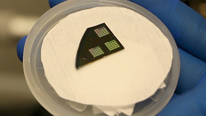
At the international IEDM 2016 conference earlier this month, Purdue University researchers revealed a number of technologies and concepts aimed at transforming tomorrow’s semiconductors. Some of the endeavors are set to boost the performance of silicon-based transistors, while others portend a path beyond silicon CMOS.
Sustaining the progress ensconced in Moore’s law over the last 50 years is top of mind to these researchers. That observation-turned-prophecy made by Gordon Moore, that transistor density on integrated circuits would double every year (revised to two years), has driven the modern era of ubiquitous computing. While transistor density may be technically on track, the benefits (smaller, faster, cheaper, more energy efficient silicon) are starting to lag as feature sizes push against the limits of physics.
Interpretations of Moore’s law aside, there is consensus that new technologies are needed to ensure continued computational progress.
“For the past 50 years, ever more electronic devices envelop us in our day-to-day life, and electronic-device innovation has been a major economic factor in the U.S. and world economy,” said Gerhard Klimeck, a professor of electrical and computer engineering and director of Purdue’s Network for Computational Nanotechnology in the university’s Discovery Park. “These advancements were enabled by making the basic transistors in computer chips ever smaller. Today the critical dimensions in these devices are just some 60 atoms thick, and further device size reductions will certainly stop at small atomic dimensions.”
Purdue researchers presented five papers during the the annual International Electron Devices Meeting (IEDM 2016), which took place Dec. 5-7 in San Francisco.
Two papers describe novel approaches for suppressing self-heating and enhancing the performance of conventional CMOS chips. The remaining papers focus on creating devices that generate less heat. Explored are networks of nanomagnets, extremely thin layers of a material called black phosphorous and “tunnel” field effect transistors, or FETs.
“There are two approaches, one is that we change the materials, use different materials or more advanced materials to replace silicon, second is we change the transistor concepts to hopefully make it much faster or energy efficient,” said Peide Ye, the Richard J. and Mary Jo Schwartz Professor of Electrical and Computer Engineering (see YouTube video below).
Ye is working to develop CMOS devices with black phosphorous. The material shows promise as a post-silicon semiconductor being capable of passing large amounts of current with ultra-low resistance while maintaining good switching performance.
Read more about this important research at http://www.purdue.edu/newsroom/releases/2016/Q4/innovations-offer-peek-into-the-future-of-electronic-devices.html.
Feature image caption: A device is made from the semiconductor germanium in research led by Purdue Professor Peide Ye (source: Purdue University image/Erin Easterling)


