Datanami
 EnterpriseAI
 HPCwire Japan
 QCwire
 HPC & AI Wall Street
Two years since announcing the industry’s first 7nm node test chip, IBM and its research alliance partners GlobalFoundries and Samsung have developed a process to build 5 nanometer (nm) chips by combining a novel switch architecture with advanced lithography techniques.
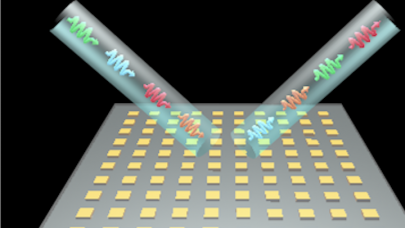
The heart of the R&D advance is a new gate-all-around architecture that employs stacked silicon nanosheets, replacing the FinFET structure used in today’s leading processors. Instead of having one single vertical fin, the horizontal “stack” can send signals through four gates, providing for better leakage control at smaller scales.
“We understood that the FinFET structure is running out of steam at 7nm and we had to invent a new device structure which could continue the scaling for several more generations,” said Mukesh V Khare, vice president at IBM Research, in an interview with HPCwire.
According to IBM, the gate-all-around architecture paves the way for fingernail-sized chips (~600mm2, says Khare) packed with 30 billion transistors—50 percent more transistors than IBM’s 7nm process enables. IBM estimates that this would provide close to a 40 percent improvement in performance for the same power or 75 percent power savings at matched performance compared with today’s leading-edge 10nm technology.
The same Extreme Ultraviolet (EUV) lithography approach that IBM used to produce the 7nm test node was applied to the nanosheet transistor architecture. With EUV, the width of the nanosheets can be adjusted continuously, within a single manufacturing process. “This adjustability permits the fine-tuning of performance and power for specific circuits – something not possible with today’s FinFET transistor architecture production,” says IBM.
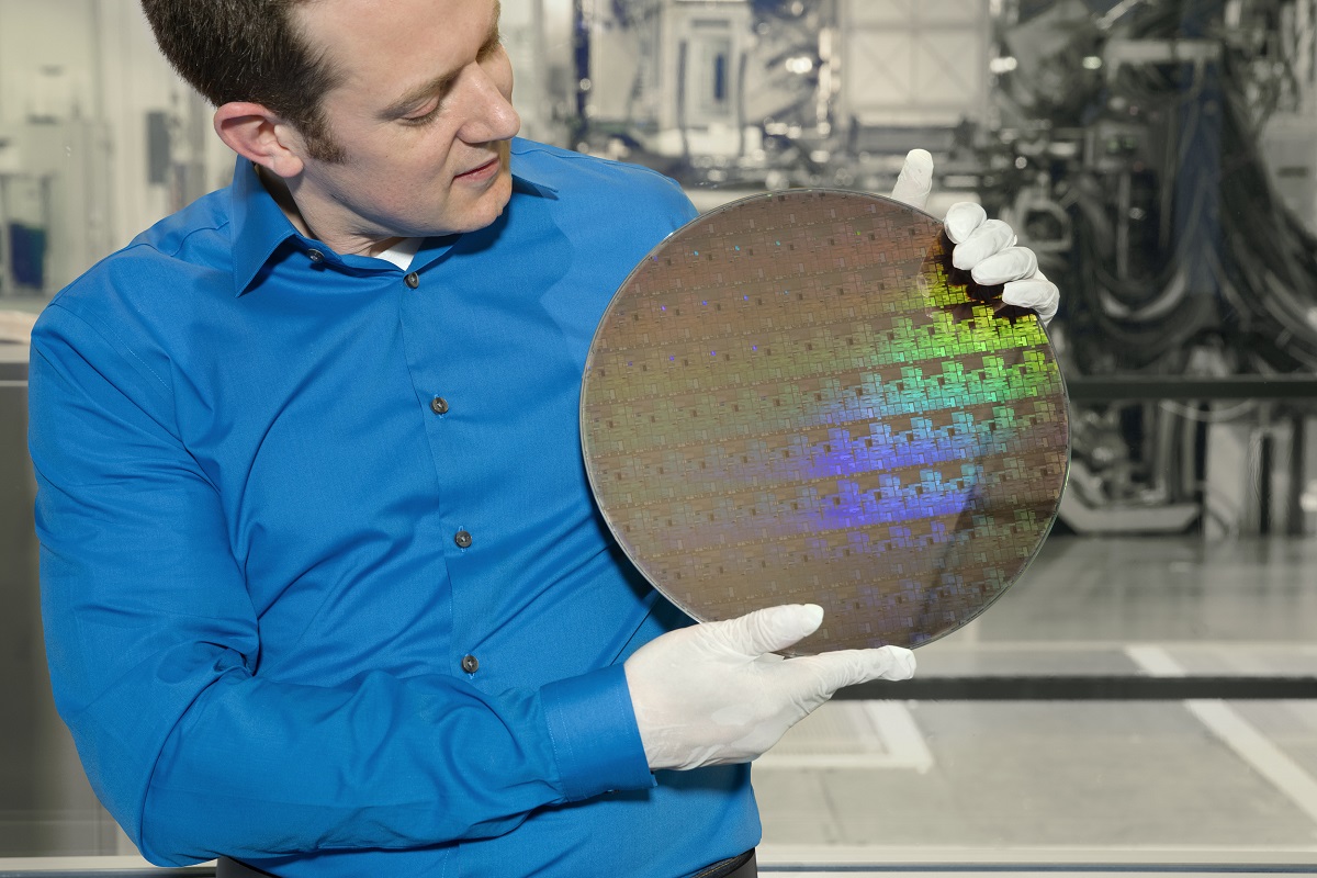
IBM and its research partners have built the transistors on 300mm wafers. “We put the entire process together, measure, validate and then our partners get full access to the technology to take it from proof point with us at IBM to manufacturing,” said Khare.
Khare emphasized, “These are not one chip or one device types of proof point; these are put together on a manufacturing scale fab which is used for research by IBM Research alliance, so this is a realistic toolset, the toolset that will eventually mature into the manufacturing toolset.”
Market analyst Jim McGregor of Tirias Research did not hesitate to call this a credible advance. “There are basically three pillars of innovation in semiconductor manufacturing,” he said. “One is the lithography process, which we’ve been completely constrained on but we’re slowly moving to EUV. The second is materials technology, which we’ve been advancing rapidly over the past decade through string silicon and other chemical makeups and the third area is transistor design. That has remained stagnant for many years, a couple decades, until we went to FinFET over the past couple years, however FinFETs are going to have their limitations architecturally and this [advance] is addressing that limitation and allows us to continue scaling, and continue basically Moore’s law. It also is injecting new materials that are going to be critical going forward, such as the the nanosheets and nanowires.”
As promising as the technical merits may be here, however, we cannot forget the economic considerations of Moore’s law, said McGregor, which will likely leave semiconductor makers like GlobalFoundries looking to leverage the FinFET technology for as long as possible to recoup the major investments that it and its partners have made. “I would estimate that at 5nm you will still see traditional FinFET,” said McGregor, “You may see IBM’s nanosheet architecture creep in later on, maybe as a sub-node to 5nm or a following process.”
IBM Research has already completed its work on the 7nm process that it introduced two years ago and transferred the technology to its manufacturing partners. IBM has said that its 7nm node will be reaching “manufacturing maturity” towards end of this year, or early next year. “The technology is very, very close,” said Khare, “and the cycle continues with another breakthrough. We will continue to work with our manufacturing partners to make this technology fully available, eventually they will decide the right timing based both on business leads as well as market drivers.”
Like the 7nm test chip before it, the latest semiconductor proof point is part of IBM’s $3 billion, five-year investment in chip R&D that was announced in 2014. As a fundamental building block for semiconductor technology, node advances will benefit all those market segments that can benefit from silicon technology scale, including high-performance computing, enterprise, and mobile. IBM, not surprisingly, is particularly focused on enhancing its cognitive computing and cloud platforms.
“Although a lot of people think of Intel when they think of semiconductor advancements, you have to remember that IBM and their development consortium accounts for a vast amount of innovation in semiconductor processing over the past 15 years or so especially,” said McGregor. “I’d say almost half of the major innovations have probably come from that alliance. It also helps push that new technology into manufacturing because these companies work so close together.”
Feature image caption: A scan of IBM Research Alliance’s 5nm transistor, built using an industry-first process to stack silicon nanosheets as the device structure (Photo credit: IBM)