Datanami
 EnterpriseAI
 HPCwire Japan
 QCwire
 HPC & AI Wall Street
GlobalFoundries has formally announced that its 7nm technology is ready for customer engagement with product tape outs expected for the first half of 2018. The global semiconductor company, headquartered in Santa Clara, Calif., says the process node offers a 40 percent performance improvement over its 14nm node, a 60 percent power reduction, and at least a 30 percent die cost reduction.
The platform integrates 17 million gates per square millimeter, over a 50 percent scaling off of 14nm. GlobalFoundries Chief Technology Officer Gary Patton noted, “Because of the need for multi patterning on these nodes, the complexity is increasing more than it has done historically. We scale a little bit more than 50 percent so when we add the higher complexity we still end up at the right point for our customers, which is at least a 30 percent die cost improvement and for some products maybe as much as 45 percent cost improvement.”
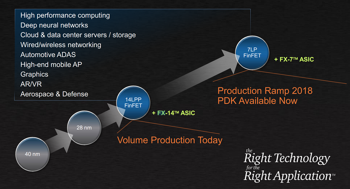
High performance computing, graphics, and networking are key areas for initial products, as are custom silicon plays. “We’re seeing a lot of push from some new players in the fabless space in the area of artificial intelligence and machine learning and they are very focused on leveraging the ASIC platform for those products.” Like Google TPUs perhaps.
GlobalFoundries has the technology to make chips up to 780 mm². Its smallest 14nm chips are around 50 mm² and some go as high as 700 mm² and it expects the same range to apply to 7nm as well.
The lack of a 10nm node on GlobalFoundries’ roadmap was strategic, a response to customer input. “I don’t personally view it as skipping a node,” said Patton, “because if you look at the density of that 10nm and performance that it offers it’s more like a half node. Our customers wanted a stronger value proposition. We made a decision two years ago to just focus on 7nm and that’s allowed us to get this offering out at this time.”
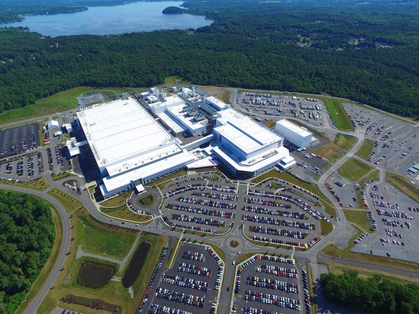
Patton views 20nm and 10nm as “weak nodes;” in contrast he sees 14nm and 7nm as having long-term staying power. GlobalFoundries has invested $12 billion in the Malta “Fab 8” factory, and is still expanding going into 2018 to support its 14nm manufacturing ramp. Having a high-yield manufacturing base on 14nm makes the development on 7nm much easier, said Patton. They’ve had over 50 designs in 14nm, and have had 100 percent first-time success on every product tape out on 14nm at the factory, according to Patton.
The 7nm process technology heads for prime time just two years after it was introduced by the IBM Research alliance which includes GlobalFoundries and Samsung. The original proof of concept chip was manufactured with extreme ultraviolet lithography (EUV), but initial products will go forward using optical lithography. This probably won’t be a surprise to those familiar with EUV’s uphill climb toward commercial viability.
EUV is progressing, said Patton, but it’s not ready for high-volume commercial production. Not wanting to hold back its customers, GlobalFoundries is launching 7nm with conventional immersion lithography and has designed the technology to be drop-in compliant with EUV. Patton expects EUV versions will be ready a year after the initial product launches – pushing that EUV goalpost into 2019.
Patton, who was with IBM for 30 years and led IBM’s semiconductor research & development organization for the last eight before the chip manufacturing business was sold to GlobalFoundries in July 2015, reviews some of the benefits EUV offers through simplification of the process. “It allows us to take some masks out, which will improve the cycle time. We can take some processing steps out which will help — the more you process wafers, the more defects you introduce, so that will give a yield advantage. We see much better line edge control with EUV and that will give some improvement in the sharpness of the features, which will give parametric advantage,” he said.
Globalfoundries Fab 8 campus in Malta, New York, has two EUV scanners arriving in 2017 and two more are scheduled for delivery in 2018. Patton says that he is encouraged by the progress that has been made on EUV, but relays four key challenge areas relating to the light source, the toolset, the resist and the mask.
“A lot of good work is being done at ASML, as well as places like IMEC, on improving mask defects, developing pellicles that would mitigate some of the defect issues, but the key challenge is being able to do that in a way that’s reliable and can withstand the high-power that’s coming out of the EUV light source – so that’s probably the long pole of the tent so to speak in getting EUV ready, but there’s good progress. We’re expecting EUV will be ready for high volume manufacturing in the 2019 timeframe and we’ll be in a position to support.”
The big takeaway is that 7nm is here and it’s on time, said Jim McGregor, founder of Tirias Research, in an interview with HPCwire. “You have to remember that on the last major process node, the 14nm, GlobalFoundries was late. It had to partner with Samsung to get moving. Since then they’ve acquired the semiconductor group from IBM and these are a lot of the same experts that developed the latest technology for the past 20 years and have really led the consortium around IBM to develop to process technologies. Now we’re seeing GlobalFoundries that was kind of trailing company in terms of rolling out new process technology moving to the forefront of being one of the leaders in rolling out new process technology.”
Synergy between IBM and GlobalFoundries was likewise emphasized by Patton. “A key part of the IBM acquisition was we take over the manufacturing of the parts, which is I think is a more efficient situation for IBM because the IBM server volumes are small,” he told us. “So we take on the manufacturing investment; we do some special things for them to make sure the technology meets their server requirements. In exchange they committed for ten years to do what they do very well, which is the fundamental research on how to keep the technology moving forward. So they continue to do the research in the IBM Watson Research Center and that pipeline of innovation flows into the Albany NanoTech center, where we do the pathfinding and determine what elements are ready for development to keep extending technology either through scaling or other creative ways.”
Moore’s law may be slowing, but it isn’t dead yet in Patton’s view. GlobalFoundries is actively investigating next-generation semiconductor technologies, such as nanowires and vertical transistors, with alliance partners IBM and Samsung at the State University of New York (SUNY) Albany NanoTech Complex, located about 30 miles south of the Fab 8 facility. You can see the fruits of their nanowire efforts in the 5nm test chip that was unveiled last week.