Datanami
 EnterpriseAI
 HPCwire Japan
 QCwire
 HPC & AI Wall Street
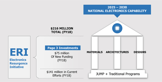
Yesterday, the Defense Advanced Research Projects Agency (DARPA) launched a giant funding effort to ensure the United States can sustain the pace of electronic innovation vital to both a flourishing economy and a secure military. Under the banner of the Electronics Resurgence Initiative (ERI), some $500-$800 million will be invested in post-Moore’s law technologies that will benefit military and commercial users and contribute crucially to national security in the 2025 to 2030 time frame.
First made public in June (see HPCwire coverage here), ERI took shape over the summer as DARPA’s Microsystems Technology Office sought community involvement on the path forward for future progress in electronics. Based on that input, DARPA developed six new programs which are part of the overall larger vision of the Electronic Resurgence Initiative. The six programs are detailed in three Broad Agency Announcements (BAAs) published yesterday on FedBizOpps.gov. Each of the BAAs correlates to one of the ERI research pillars: materials and integration, circuit design, and systems architecture.
Also joining the ERI portfolio are several existing DARPA programs (including HIVE and CHIPS) as well as the Joint University Microelectronics Program (JUMP), a research effort in basic electronics education co-funded by DARPA and Semiconductor Research Corporation (SRC), an industry consortium based in Durham, N.C.
DARPA says that with the official roll out of the Electronics Resurgence Initiative, it “hopes to open new innovation pathways to address impending engineering and economics challenges that, if left unanswered, could challenge what has been a relentless half-century run of progress in microelectronics technology.”
DARPA is of course referring to the remarkable engine of innovation that is Moore’s law. Gordon Moore’s 1965 observation that transistor densities were doubling at roughly 24-month intervals set the stage for five decades of faster and cheaper microelectronics. But as node feature sizes approach the fundamental limits of physics, the design work and fabrication becomes ever more complex and expensive, jeopardizing the economic benefits of Moore’s dictum.
It’s something of a grand experiment, explained Bill Chappell, director of the Agency’s Microsystems Technology Office (MTO) in a press call, referring to the scale and scope of the Electronics Resurgence Initiative. DARPA has packaged up into one large announcement six different programs (released in three Broad Agency Announcements – BAAs — on FBO.gov). The six different programs will in sum receive $75 million in investment over the next year alone and on the order of $300 million over four years. Like all DARPA programs, the longevity and funding levels of these programs will be tied to performance.
“If we see that we’re getting broad resonance within the commercial industry and within the DoD industry, and unique partnerships are forming and/or unique capabilities are popping up for national defense, it will continue with the expectation or even grow,” said Chappell.
The DoD is finding it increasingly difficult to manufacture and design circuits, partly due to Moore’s law slowdowns and partly due to the scale of designs. “We are victim of our own success in that we have so many transistors available that we now have another problem which is complexity, complexity of manufacturing and complexity of design,” said Chappell. “So whether Moore’s law ends or not, at the DoD, from a niche development perspective we already have a problem on our hands. And we’re sharing that with the commercial world as well; you see a lot of mergers and acquisitions and tumult in the industry as they try to also grapple with some of the similar problems and the manpower required to get a design from concept into a physical product.”
Here’s a rundown on the six programs organized by their research thrust:
Materials and Integration (link)
- Three Dimensional Monolithic System-on-a-Chip (3DSoC): Develop 3D monolithic technology that will enable > 50X improvement in SoC digital performance at power.
- Foundations Required for Novel Compute (FRANC): Develop the foundations for assessing and establishing the proof of principle for beyond von Neumann compute topologies enabled by new materials and integration.
Design (link)
- Intelligent Design of Electronic Assets (IDEA): “No human in the loop” 24-hour layout generation for mixed signal integrated circuits, systems-in-package, and printed circuit boards.
- Posh Open Source Hardware (POSH): An open source System on Chip (SoC) design and verification eco-system that enables cost effective design of ultra-complex SoCs.
Novel Computing Architectures (link)
- Software Defined Hardware (SDH): Build runtime reconfigurable hardware and software that enables near ASIC performance without sacrificing programmability for data-intensive algorithms.
- Domain-Specific System on Chip (DSSoC): Enable rapid development of multiapplication systems through a single programmable device.
Chappell gave additional context for the Software Defined Hardware program, noting that it will look at course-grained reprogrammability specifically for big data programs. “We have the TPU and the GPU for dense problems, for dense searches, and dense matrix manipulation. We have recently started the HIVE program, which does sparse graph search. But the big question that still exists is what if you have a dense and sparse dataset? We don’t have a chip under development or even concepts that are very good at doing both of those types of datasets.”
What DARPA is envisioning is a reprogrammable system, or chip, that is intelligent enough and has an intelligent enough just in time compiler to recognize the data and type of data it needs to operate on and reconfigure itself to the need of that moment. DARPA has done seedlings to demonstrate that it’s feasible but “it’s still a DARPA-hard concept to pull off,” said Chappell.
DARPA will hold a number of Proposers Days to meet with interested researchers. The FRANC program of the Materials and Integration thrust will be run in the form of a webinar on Sept.15 and that thrust’s other program, 3DsoC, will take place at DARPA headquarters in Arlington, Va., on Sept. 22. The Proposers Day for the Architectures thrust’s two programs, DSSoC and SDH, will take place near DARPA headquarters in Arlington, Va., on Sept. 18 and 19, respectively. The Proposers Days for both programs in the Design thrust—IDEA and POSH—will take place on Sept. 22, in Mountain View, Calif. Details about all of these Proposers Day events and how to register are included in this Special Notice, DARPA-SN-17-75, posted on FBO.gov.
Asked about the goals for ERI writ large, Chappell said, “Overall success will look like we’ve invented the ideas that will be part of that 2025 and 2030 electronics community in such a way that both our defense base has better access to technology, better access to IP, better design services and capabilities than they have today because of these relationships that we are trying to build while simultaneously US interests in electronics in regards to economic development, maintaining our dominant global position is secured because of the new ideas that we are creating through these investments.
“These $75 million next year and $300 million over the course of the next four years that we’re planning is for very far-out research which often times is not something that a commercial entity can do because of its speculative nature and/or not something the DoD can do because it isn’t necessarily solving a today problem, but a tomorrow problem.”
DARPA is known for funding high-risk, high-reward R&D with broad commercial impact, helping to invent both the Internet and GPS.