Datanami
 EnterpriseAI
 HPCwire Japan
 QCwire
 HPC & AI Wall Street
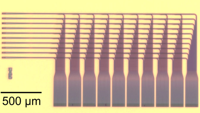
Researchers at the National Institute of Standards and Technology (NIST) have made a silicon chip that distributes optical signals precisely across a miniature brain-like grid, showcasing a potential new design for neural networks. The work also represents an important advance in the ability to create denser, complicated photonic circuits, which is a critical need for integrating photonics with other circuits.
“In a system with both photonic and electronic components, the chip area consumed by photonics grows rapidly as the number of communicating nodes, and their degree of connectivity, is increased. For densely connected systems, the requisite number of waveguides can increase to the point where they cannot fit on one plane,” observe the researchers in their paper published last week in APL Photonics.
“A suitable solution is the use of multiple planes of photonic waveguides, a field which has seen significant progress over the last decade. The stacking of waveguides allows for dense integration with low-loss and low-cross talk waveguide crossings. In the present work, we present the design and implementation of a two-plane signal distribution network routing 10 input nodes in one network layer to 100 connections on 10 output nodes. This routing manifold accomplishes the routing between two layers of a feed-forward neural network with 10 neurons per layer and all-to-all connectivity.”

An account of the work (NIST Chip Lights Up Optical Neural Network Demo) is also posted on the NIST web site. The three-dimensional (3D) design used enables complex routing schemes, which are necessary to mimic neural systems. Furthermore, say the researchers, this design can easily be extended to incorporate additional waveguiding layers when needed for more complex networks.
Neural networks already have demonstrated remarkable power in solving complex problems, including rapid pattern recognition and data analysis. The use of light would eliminate interference due to electrical charge, and the signals would travel faster and farther.
“Light’s advantages could improve the performance of neural nets for scientific data analysis such as searches for Earth-like planets and quantum information science, and accelerate the development of highly intuitive control systems for autonomous vehicles,” said NIST physicist Jeff Chiles in the NIST article.
“We’ve really done two things here. We’ve begun to use the third dimension to enable more optical connectivity, and we’ve developed a new measurement technique to rapidly characterize many devices in a photonic system. Both advances are crucial as we begin to scale up to massive optoelectronic neural systems.”
Link to paper (Design, fabrication, and metrology of 10×100 multi-planar integrated photonic routing manifolds for neural networks): https://aip.scitation.org/doi/10.1063/1.5039641
Link to NIST article: https://www.nist.gov/news-events/news/2018/07/nist-chip-lights-optical-neural-network-demo
Source: NIST