Datanami
 EnterpriseAI
 HPCwire Japan
 QCwire
 HPC & AI Wall Street
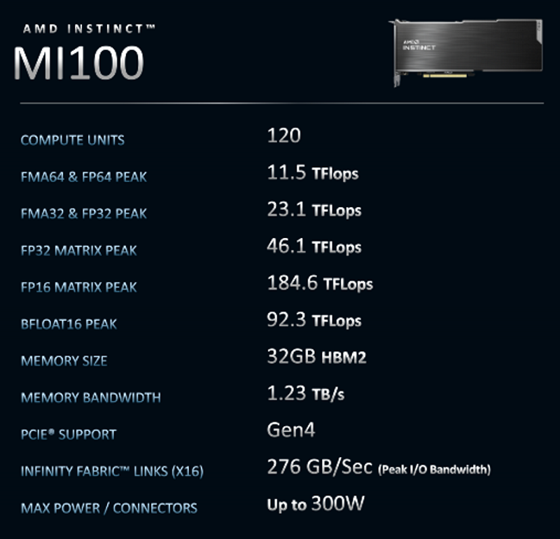
AMD today announced the new MI100 Instinct accelerator, billing it as “the world’s fastest HPC GPU” with 11.5 teraflops of peak double-precision floating point performance. A follow on to the MI50 and MI60 Instinct accelerators launched two years ago (the “world’s first 7nm datacenter GPUs”), the MI100 is also manufactured on TSMC’s 7nm process, but boasts twice as many compute units as the previous generation within the same 300-watt power envelope.

The MI100 GPU is the first to incorporate AMD’s Compute DNA (CDNA) architecture with 120 CUs organized into four arrays. An evolution of AMD’s earlier GCN architecture, CDNA includes new matrix core engines that boost computational throughput for different numerical formats.
Going down the spec sheet, the MI100 offers 46.1 teraflops peak single-precision matrix (FP32), 23.1 teraflops peak single-precision (FP32), 184.6 teraflops peak half-precision (FP16) floating-point performance, and 92.3 peak teraflops of bfloat16 performance.
The new AMD matrix core technology provides the MI100 with 7x greater peak half-precision floating point performance compared to the MI50, according to AMD. Brad McCredie (corporate vice president of datacenter GPU and accelerated processing at AMD) told HPCwire the company is exploring other emerging numerical formats that target AI and ML workloads, but doesn’t want to get too far out in front of the industry.
AMD’s MI100 GPU presents a competitive alternative to Nvidia’s A100 GPU, rated at 9.7 teraflops of peak theoretical performance. However, the A100 is returning even higher performance than that on its FP64 Linpack runs. (Yes, you heard right.) The A100 GPU is achieving ~12 double-precision Linpack teraflops (see Selene, for example), and Nvidia confirmed to me they use a different double-precision peak for their marketing material and for their Top500 rMax (9.7 versus 15.1 teraflops, respectively).
As new numerical formats optimized for AI/ML gain traction, performance comparisons – already a challenging, if not dark, art – are becoming more confounding. As always the only sound comparisons rest on cost-performance and real-world evaluations for real-world applications. While prices for the MI100 have not been publicly disclosed and Nvidia does not advertise a list price for its A100s, AMD is claiming a 1.8x to 2.1x flops-per-dollar advantage over its competitor.

Implementing the second-generation AMD Infinity Fabric Technology, AMD says the MI100 provides ~2x the peer-to-peer peak I/O bandwidth over PCIe 4.0 with up to 340 Gbps of aggregate bandwidth per card. AMD’s bridging device (see graphic) joins four MI100 PCIe cards into a single coherent scale-up solution. In a server, the MI100 GPUs can be configured with up to two integrated quad GPU hives, each providing up to 552 Gbps of peer-to-peer I/O bandwidth, according to AMD.
“We did four cards [fully-linked] because we think that is the sweet spot for HPC deployments, this four-to-one GPU to CPU ratio,” said McCredie.
Four stacks of 8GB HBM2 memory provide 32GB HBM2 memory on each MI100 GPU. At a clock rate of 1.2 GHz, that’s 1.23 Tbps of memory bandwidth. As with the MI50, the MI100’s support for PCIe Gen 4.0 technology enables 64 Gbps peak theoretical transport data bandwidth between CPU and GPU.
AMD said it has no plans for custom mezzanine form factors with this generation – but AMD does see a role for those form factors going forward as you might expect given their exascale wins (Frontier and El Capitan). While detailed node structures have not been publicly disclosed, both of these designs employ a four-to-one GPU to CPU ratio.

HPC market watcher Addison Snell, CEO of Intersect360 Research, remarked on AMD’s HPC focus and the implementation of its datacenter-centric CDNA architecture, distinct from the gaming-oriented RDNA (Radeon DNA) architecture.
“With the MI100 GPU, AMD is staying pure to its corporate focus on HPC,” said Snell. “While Nvidia’s messaging and benchmarking have been AI-heavy, AMD is hitting HPC hard, with 11.5 teraflops of double-precision performance as the marquee stat.”
“AMD is also emphasizing its new CDNA architecture as the focus for computing versus graphics; that’s where we find the GPU-to-GPU communication on the second-generation Infinity architecture.”
Prominent HPC sites Oak Ridge National Laboratory, the University of Pittsburgh and Pawsey Supercomputing Center evaluated the new GPUs along with AMD’s software frameworks. Their reports are positive.
“We’ve received early access to the MI100 accelerator, and the preliminary results are very encouraging. We’ve typically seen significant performance boosts, up to 2-3x compared to other GPUs,” said Bronson Messer, director of science, Oak Ridge Leadership Computing Facility. “What’s also important to recognize is the impact software has on performance. The fact that the ROCm open software platform and HIP developer tool are open source and work on a variety of platforms, it is something that we have been absolutely almost obsessed with since we fielded the very first hybrid CPU/GPU system.”

AMD is preparing ROCm – its open source toolset consisting of compilers, programming APIs and libraries – to be foundational for exascale computing. The recently released ROCm 4.0 has upgraded the compiler to be open source and unified to support both OpenMP 5.0 and HIP, said AMD. HIP (AMD’s heterogeneous-compute interface for portability) is a C++ runtime API that allows developers to write single-source code that can run on AMD and Nvidia GPUs (and possibly future Intel ones as well).
AMD reported that MI100-based systems will start shipping this month from a number of partners, among them Dell, Gigabyte, Hewlett Packard Enterprise and Supermicro.