Datanami
 EnterpriseAI
 HPCwire Japan
 QCwire
 HPC & AI Wall Street
Intel announced it is investing $3.5 billion in its Rio Rancho, New Mexico, facility to support its advanced 3D manufacturing and packaging technology, Foveros. The Rio Rancho site is where Intel currently develops and manufactures its next-generation Optane memory technology as well as its embedded multi-die interconnect bridge (EMIB) and silicon photonics technologies. Planning activities are to commence immediately, according to Intel, with construction expected to start later this year.
At an on-site news conference held this morning, Intel said the facility is being upgraded to support the development of Foveros, its 3D packaging technology that allows compute tiles (Intel-speak for chiplets) to be stacked vertically, rather than side-by-side. Together with EMIB, Foveros enables a mix and match approach, uniting different types of tiles on the same package. The move from system-on-chip to system-on-package is key to satisfying the computational demands of the modern datacenter, as well as edge and 5G, Intel said.
Intel’s advanced packaging technologies EMIB and Foveros have been implemented in Ponte Vecchio, the company’s future datacenter GPU, scheduled to debut in the Aurora supercomputer at Argonne National Laboratory in 2022. Ponte Vecchio consists of 47 “XPU” tiles integrated into a single package.
The $3.5 billion multiyear investment will expand the footprint of the Rio Rancho campus by roughly 40 percent. In partnership with New Mexico state and local government, the modernization project is expected to create 1,000 construction jobs, 700 permanent high-tech positions and support 3,500 in-state jobs once the project is complete. Intel currently employs more than 1,800 people at the Rio Rancho site.
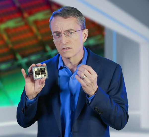
The investment is good news for New Mexico and the Rio Rancho facility, which was showing signs of its age, said Jim McGregor, principal analyst and founder at TIRIAS Research. “It’s good that [this upgrade] keeps the jobs there and that Intel’s going to continue investing in Rio Rancho, rather than just being a limited facility. Plus it shows Intel is continuing to make investments under new CEO Pat Gelsinger.”
This latest move follows Intel’s $20 billion plan to build two new Arizona fabs as part of the company’s IDM 2.0 strategy, announced by Gelsinger in March. Under IDM 2.0, Intel is investing in and leveraging its internal factory network, expanding its use of partner capacity and establishing Intel Foundry Services.
McGregor expects that Intel, guided by its IDM 2.0 playbook, will be making investments not only in fab capacity for fabrication of silicon, but also in back-end assembly. “They’re going to continue investing across the board so that they not only make sure that they have their own capacity, but also be that they become a world-class foundry,” he told HPCwire.
At today’s live-streamed media event, Keyvan Esfarjani, Intel senior vice president and general manager of manufacturing and operations, said that semiconductors are the fifth largest U.S. export sector, supporting more than one million jobs directly and another million ancillary jobs in the U.S. “But there’s room to grow this industry further here in United States,” he said, “for companies to capture more of the domestic share as well as support the supply chain across our global operations.”
Intel is positioning the New Mexico facility as a critical domestic hub for advanced semiconductor manufacturing. The company is hoping the large outlays it is making in its manufacturing capabilities will help it secure funding from both the U.S. and E.U. governments.
Intel’s end game is to restore its leadership manufacturing performance. Delays and setbacks for Intel’s roadmap have allowed rivals TSMC and Samsung to gain a two-to-three year advantage in process technology. Intel CEO Gelsinger acknowledges the lag, but is bullish about a comeback.
“We believe it’s gonna take us a couple of years and we will be caught up [to TSMC],” he told CBS’s 60 Minutes in a segment that aired Sunday night.

What about Optane?
While the Rio Rancho campus manufactures next-generation Optane technology, the upgrade project that was announced today does not commit additional funds for 3D XPoint/Optane fabrication. Since Micron exited the 3D XPoint business and put the primary fabrication facility (in Lehi, Utah) up for sale, Intel has yet to disclose how it will be sourcing 3D XPoint memory chips in the future. Analysts we spoke with say it’s more likely that Intel will acquire an existing fab or build from scratch rather than retrofit an existing facility.
“When you build a fab for a purpose, whether it’s for memory, for logic, or back-end assembly, you have to build it for the intended purpose to get the maximum use out of it and return on investment,” said McGregor. “We may think $3.5 billion is a lot of money, but it’s really not that much. Quite honestly, that’s barely enough to retrofit the equipment in a facility — that doesn’t even include a new (purpose-built) facility.”
Buying Micron’s Lehi facility makes more sense, according to Jim Handy, principal at Objective Analysis.
“I’ve always thought it would be cheapest for Intel to take over the Lehi fab and tell everyone ‘keep doing what you’re doing.’ That seems like a slam dunk for Intel and they haven’t done it yet, which I find kind of shocking. Moving production 3D XPoint fabrication to Rio Rancho would require sizable investments,” Handy told HPCwire.