Datanami
 EnterpriseAI
 HPCwire Japan
 QCwire
 HPC & AI Wall Street
At yesterday’s Quantum in Industry session at the APS March Meeting 2022, Google, IBM, Intel, Quantinuum, and Silicon Quantum Computing/University of South Wales (USW) presented progress points and ongoing challenges in the race to achieve practical quantum computing. While IBM has proclaimed 2023 to be the year it achieves quantum advantage, the other participants expressed more modest views on when QA will be achieved, but offered positive views on progress in solving underlying quantum technology challenges.
The APS.org March Meeting has become a key forum for quantum computing-related research, and in recent years, many of commercial companies have multiple presentations. Google, for example, has at least six other presentations at MM this year. IBM pitched its QV benchmark here in 2019 and QV has since been adopted by a few others. Presentations at the March Meeting tend to be granular and feature results from recent work. The Quantum in Industry invited talks typically straddle between overview and deep dive with elements of each.
Google reprised its overall strategy and timeline and then dug deeper into its error correction research and roadmap. USW/Silicon Quantum Computing discussed advances in manufacturing single-atom qubits in silicon that offer scaling and performance advantages. IBM largely reviewed work it had discussed at its user conference in December. Intel continued emphasizing its ability to leverage CMOS manufacturing expertise for fabbing quantum dot qubits; it also provided more detail around an impressive new cryogenic wafer prober. Quantinuum, the lone ion trap presenter, examined advances in basic architecture, ion transport, logical gates, and qubit initialization and detection.
The ever-present question of when we will have error-corrected quantum computers drew a range of estimates – a Google slide showed 2029; a USW/SQC slide suggested 2033, and an IBM slide indicated 2026-plus. There seemed to be more consensus that systems able to produce quantum advantage for a few applications may begin appearing sooner.
This year’s March Meeting is a hybrid in-person/virtual event. The industry session was chaired by Andrew Cleland, a quantum researcher at the University of Chicago, and there’s a recorded video (registration may be required) of the all of the presentations. Presented here is a small portion of Google’s comments on its approach to error correction, along with a few highlights from the other talks. (My Zoom quality was intermittent for the Quantinuum presentation so that talk is not included). As always with quantum topics, it’s best to watch the presentations directly.
Google Attacking Error Correction and Scaling
Google, of course, is betting on superconducting qubits. As with all qubit technologies, a variety of system and random noise is a huge problem and causes unacceptable error rates. One approach is to use so-called surface codes for error correction but doing so isn’t trivial and requires overhead. Kevin Satzinger, a research scientist at Google Quantum AI, spent some time in his talk on Google’s efforts with surface codes (also sometimes called distance codes).
“For the algorithms that we all dream of running on our quantum computers, they require error rates of perhaps 10-10 to 10-12 in order to get the results that we need. While modern hardware [has] typical error rates approaching perhaps 10-3, which is several orders of magnitude [difference] – quite the chasm in error. The bridge to span that chasm is quantum error correction,” said Satzinger. “The idea is to create logical qubits where we distribute the logical information across an array of qubits, we’re paying attention to the surface code here.”
“So, it would be an array of d squared physical qubits, the blue qubits here, where d is the code distance and by distributing the quantum information like this, we can make it immune to local errors. But it comes at a cost because we have a bunch of extra stuff, a bunch of overhead, and a bunch of extra operations that we have to do in order to carry out the error correction. And because of that overhead, if your components are not performing well enough, it is possible that you’re doing more harm than good by doing all of this extra error correction stuff,” he said.

There’s a breakeven point, said Satzinger, where error correction starts “helping you out.”
“That (breakeven) concept is related to the threshold,” he said. “Let’s consider this expression at the bottom of the slide (above) where the error per logical gate is proportional to this ratio, the error per physical gait, divided by an error correction threshold raised to this power in the code distance. If this quantity, one over Lambda is a small number, you’re raising it to a power in the code distance, [and] you can exponentially reduce the logical error. That’s exactly what we need in order to cross that chasm of orders of magnitude.”
“But this one over lambda really matters for what overhead you’re going to require. For example, consider the case where you want this right-hand side (see slide) here to be 10-12. Well, in that case, we can look at a particular value of one over Lambda and compute for the surface code how many physical qubits would we need for one logical qubit. If lambda equals one, you’ve barely reached breakeven, and the quantity diverges.”
Satzinger noted that as you improve performance, moving to the left on the plot (slide above), the resource requirements drop dramatically, down to about one-thousand physical qubits per logical qubit at lambda equals 10. “That is our target for the time being. With that context, I can now elaborate a bit more on our two upcoming milestones. The first one is to build a logical qubit prototype. And the idea here is to build a device where we can run a distance three surface code, and a larger distance five surface code and compare their performance. The goal for the distance five surface code to be better than the distance three in terms of logical error is quite challenging,” he said.

There’s been a good deal of work in the community around distance codes for use in quantum error correction.
“I would remark that there’s often kind of a criticism of these distance three codes, that comes from a comparison between the physical qubits’ coherence time, and the effective logical coherence time of the distance three, logical qubit. But you know what, I don’t mind one bit if a logical qubit of distance three has a shorter lifetime than the physical qubits. It would be great if it did have a longer lifetime. But consider this example: you could have a large error corrected quantum computer with glorious 10-12 errors and have it still be the case, depending on the particular parameters, that if you made a distance three code on that device, that itself would not have a longer lifetime than the physical qubits, so it doesn’t really matter,” said Satzinger.
“In contrast, the scaling behavior is critical. If we can’t get bigger to be better than the whole enterprise won’t work. And so that’s why we’re focusing on this scaling comparison of looking at a distance three and a distance five code and trying to get as good performance as we can to get better performance so that the distance five isn’t, in fact, better than the distance three, which will require significantly better performance than what has been published,” said Satzinger.
Silicon Quantum Computing/USW – Single Atom Qubits in Silicon
Michelle Simmons, founder and director of start-up Silicon Quantum Computing and long-time, prominent researcher in quantum physics and condensed matter, discussed USW/SQC’s steady work to understand and develop techniques to create single atom qubits (phosphorous) in silicon. Working with scanning tunneling microscopy (STM), she and her team are able to precisely fab and align these single atoms. They have also developed nanowire technology.
Simmons is the winner of 2022 American Physical Society Beller lectureship, which funds distinguished physicist from abroad to give invited talks at APS meetings. Her talk, Manufacturing qubits in silicon with atomic precision, was fascinating. She and collaborators have gone so far as to image the electron ‘position’ which she says turned out not to be fuzzy. “Most people think that electron cloud around a donor atom is roughly like a kind of fuzzy ball. But in reality, you can go in with the STM tip, and you can actually image directly what the wave function looks like. And this is a very powerful tool because it tells you where the electron sits within the crystal,” she said.
“We’ve really figured out how to deterministically put dopants in silicon crystal surface, how to connect them with lead states, how to measure where they are, create sensors that we can come in and do the spin states. You can get single shots read out, be able to do spin transport through these devices, look at the metrology of where they sit, independently read them out, and then basically get to the point where we’re starting to get single qubit gates of high quality. We can RF couple them. We found that these wires are very low capacitance because they’re monolayer thick, so you get little crosstalk between them in the surface. And because they’re very small, you can get very high fidelity readout. We’ve got fast two-qubit gates, we’ve figured out how to benchmark the readout so we can optimize it using our devices looking at cavity coupling, coherent control,” said Simmons.

IBM – Circuit Knitting to Improve Performance
IBM showcased steady advances in severaL areas (hardware, software, tools) with IBM quantum researcher Hanhee Paik handling the presentation. She looked briefly at the near-term agenda. IBM was an early entrant to the quantum computing arena and currently has 24 quantum systems of various sizes online. Its roadmap calls for delivering a 433-qubit system this year and 1000-plus-qubit system in 2023.
Paik emphasized the ongoing need for materials research as needed enablers for advances in working cold temperatures. She also cited IBM work on creating user-friendly environments such as its serverless architecture.


Intel – Cryogenic Wafer Probe Speeds Throughput and Feedback
Central to Intel’s thrust into quantum computing is the idea that leveraging its tremendous CMOS manufacturing expertise will enable it to get to scale faster.
In what was one of the more intriguing comments during the session, Otto Zeitz, a quantum hardware engineer at Intel, said, “You know Intel ships over 800 quadrillion transistors every year. And by 2025, it’s expected that there’ll be more transistors on Earth than human cells. This is just a massive number of devices that are being fabricated and then delivered out and being used in the community. And it turns out that [Intel’s] silicon spin qubit devices are very similar to these transistors.”
He said little new about the actual fab process for its quantum dot qubits, which Intel has long said uses its existing 14nm process line. Intel creates it dot qubits with silicon-germanium on silicon technology. More interesting and fresher news was Intel progressing in evaluating its wafers.
Consider the process for regular transistors. Intel produces about 10,000 devices on 300mm wafers. “Traditionally, our process flow would look like a wafer would come out, and you would do room temperature characterization and this is very similar to what we do in our advanced CMOS line in our HBM processes. And here, you can get transistor metrics in about two hours across the wafer looking at thousands of devices,” said Zeitz.
“As we start to move into the spin qubit space, the information that we’re interested in is really more relevant at cryogenic temperatures. In a silicon-germanium/silicon device, you’re forming your junction at the interface of that buried silicon well, so you don’t have any information about that today at room temperature, and you need to go to lower temperatures to really characterize your quantum dot characteristics. This is performed through our quick turn fridges and they’re approximately 1.6 Kelvin. We can dice, package, and load an individual device from across the wafer, and then measure it in about 12 hours. It takes about 12 hours to measure each device. Then we can sample across the wafer individually to get an idea of performance across the wafer. Then we can move our most promising devices into our dilution refrigerators, where qubit formation and cubic characterization is taking place,” said Zeitz.
Intel worked with its supplier Bluefors to develop a cryo wafer probe which Zeitz said is now commercially available from Bluefors.
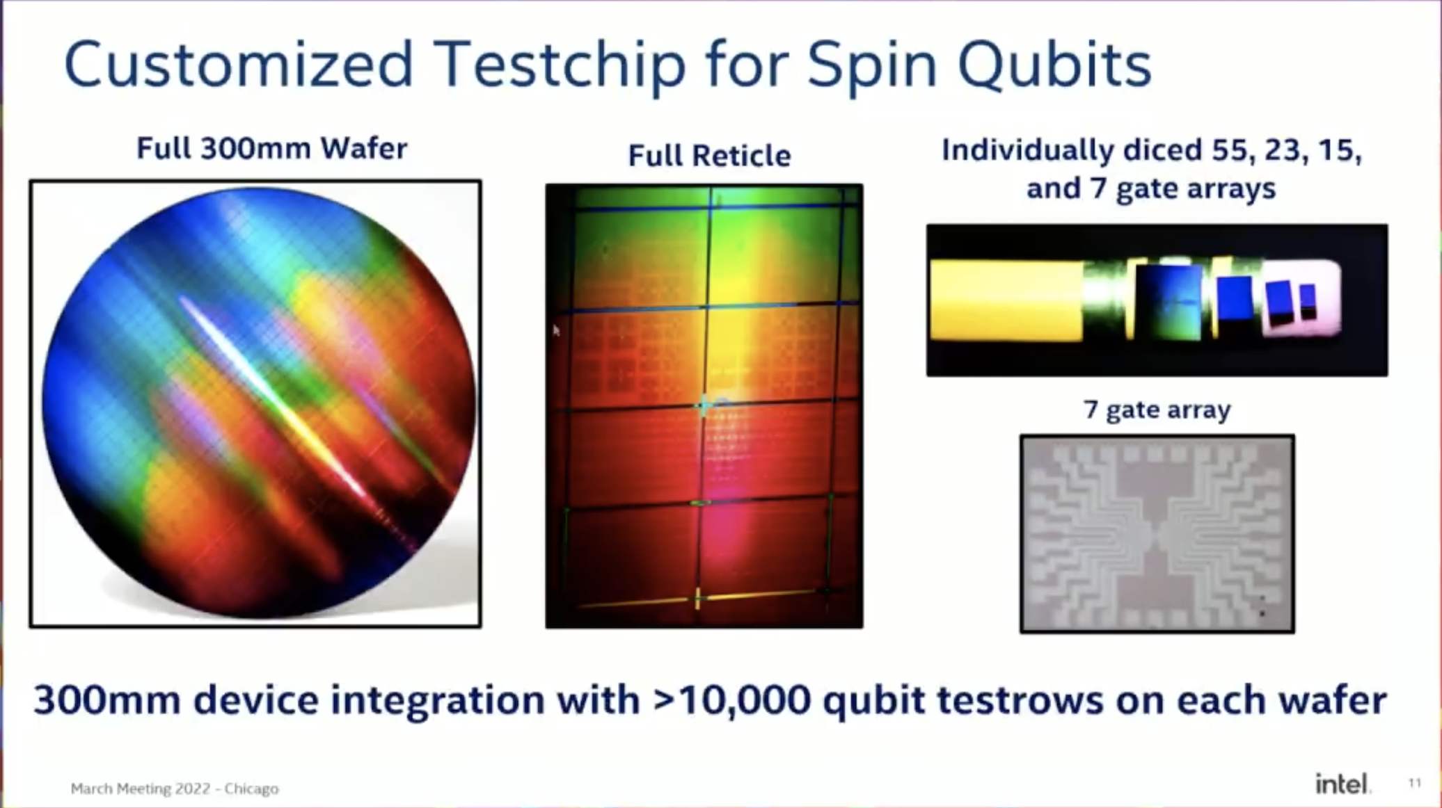

“This tool actually came at the very beginning of the pandemic, and we were able to install it and start collecting data throughout this time. Briefly, the way the system works is you have these two cooling systems from Bluefors attached to a vacuum system from Afore (vacuum chamber) and inside of this system is your probe card and your wafer and your stage which allows you to move across the wafer. Additionally, this system has a load lock, and this load lock lets us transfer wafers into the system without significantly warming it up. It takes about two hours from the time a wafer comes out of our R&D fab, and I’ve placed it in this tool until I can start collecting information below to Kelvin and start getting that relevant quantum dot and low temperature physics information.”
Link to APS.org: https://www.aps.org