Amid the high-performance GPU turf tussle between AMD and Nvidia (and soon, Intel), a new, China-based player is emerging: Biren Technology, founded in 2019 and headquartered in Shanghai. At Hot Chips 34, Biren co-founder and president Lingjie Xu and Biren CTO Mike Hong took the (virtual) stage to detail the company’s inaugural product: the Biren BR100 general-purpose GPU (GPGPU).
“It is my honor to present our first-generation compute product: BR100,” Xu said. “BR100 is dedicated to addressing the challenges of AI training and inference in the datacenter, with augmented goals of increasing productivity and reducing overall cost of ownership.”

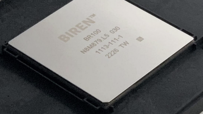
At 1074mm2, the 77 billion-transistor, dual-die Biren BR100 (pictured in the header) will be manufactured on TSMC’s 7nm process and capable of 256 FP32 teraflops. The die-to-die interconnect provides 896GB/s bandwidth. The BR100 comes with up to 64GB of HBM2E memory (across four stacks) and can manage up to 2.3TB/s in external I/O bandwidth among its octuple BLink connections. All of this adds up to a max TDP of 550W and a targeted clock frequency of 1GHz.
Given the BR100’s targeted use cases, the point of comparison was no surprise: Nvidia’s A100 GPU, which has become the de facto reference point in the widening field of accelerators. The BR100’s peak teraflops, of course, compare extraordinarily favorably to the A100 — 19.5 for the A100, 256 for the BR100 (“one of the fastest GPUs in the world,” Xu said). Beyond the flops, Xu said they had seen promising results on workloads and benchmarks.
“Compared with the Nvidia A100, at the current stage, we see an average of 2.6(×) speedup over a broad range of benchmarks across different domains, including computer vision, natural language processing and conversational AI,” he said. “Performance will continue to go up in the coming months as we keep optimizing hardware and software.”

“We had two design goals for the BR100,” Hong said. “The first: it needs to reach one petaflops horsepower. The second: it should be a GPGPU, not a pure AI accelerator.”
With that, let’s return to flops for a moment: the BR100 supports FP32, BF16, FP16, INT32, INT16 and other formats — but there are two additional points of note: first, the BR100 does not support FP64 (“We decided to dedicate chip area to our targeted markets and use cases,” Xu commented); second, the BR100 does support a new 24-bit data type called TP32+. And, with 1024 teraflops of performance at BF16, it looks like the BR100 fits Biren’s bill of “one petaflops horsepower.”
The BR100 will also come in another flavor: the BR104, a single-die variant designed for use in PCIe cards. Xu said that Biren is also working with manufacturers to build reference cluster designs. The chip itself has already been tested on real silicon. What’s more: “We already submitted to the latest round of MLPerf inference, and you should be able to see our results in two or three weeks,” Xu said. (Biren a member of MLCommons.)

Biren Technology jointly released the 8-way Hearten OAM server in partnership with Inspur. The companies expect to begin sampling the hardware in the fourth quarter of this year.
Devices will ship with Biren’s own software platform and programming model, called BIRENSUPA. “Developers who are familiar with (Nvidia’s) CUDA can easily write code for SUPA,” said Hong. Supported AI frameworks include PyTorch, TensorFlow and PaddlePaddle. The company also provides the OpenCL compiler. The dual-die BR100 appears as one GPU to the software layer.
As of its Series B funding round, Biren has raised more than 5 billion CNY (~$730 million USD).

