Datanami
 EnterpriseAI
 HPCwire Japan
 QCwire
 HPC & AI Wall Street
Optical I/O is being singled out by top companies to push computing beyond exascale and into zettascale. The technology was singled out in a recent speech by AMD CEO Lisa Su as a critical technology to reach zettascale computing from both a power and performance perspective.
“Optical communication is a key area that we think is very, very important for us to reach anything like zettascale type of computing capability,” Su said.
Optical communication has been used for decades, largely in telecommunications, to speed up transmission over long distances. The hardware so far has required pluggable modules to transmit and receive signals, as the data travels over long distances from one point to another.
But chipmakers are now bringing optical I/O closer to the chip layer for short-distance communications in supercomputers and datacenter infrastructure. For example, optics could be used to link up GPUs in close range.
AMD is working with DARPA on packaging optics solutions into chips, Su said.
Intel, which uses technologies like Ethernet and InfiniBand, also sees silicon photonics as integral to its zettascale plans. Intel is bringing optical on-package to address bandwidth, energy efficiency in its future chip designs based on chiplets, in which computing cores can be patched together like modules.
Intel’s current supercomputing GPU called Ponte Vecchio has a technology called XE Link, which is a tile that provides a communication link between GPUs.
“Some of those will be upgradeable to optical I/O,” said Jeff McVeigh, the corporate vice president and interim general manager of the Accelerated Computing Systems and Graphics Group at Intel, in a press conference last year.

Broadcom is also chasing optical interconnects on chiplets. The company, which is a recent entrant into the optical I/O space, earlier this month announced a more deeply integrated optical I/O that could communicate at 51.2 terabits per second.
The computing density is becoming tighter and tighter, and optical I/O provides the hooks for faster and more energy efficient GPU-to-GPU communications, which is demanding with AI/ML operations.
“Let’s say if you take a direct-attached copper cable operating at 100G, it has a certain bend radius which limits how you want to put two boards as close as possible together. There fiber optics provides better bend radiuses, tighter density, and tighter integration,” said Vivek Raghuraman, director of research and development at Broadcom, in an interview with HPCwire.
If there is a copper-based solution that can meet a certain cost point, then datacenters are going to try and use that. But performance metrics in applications like machine learning could ultimately pave the way for high-density integration and optical I/O to connect GPUs.
“We are seeing this is in high-density integration where it’s becoming more and more the use case, and we are working on those platforms – like ML GPU to GPU – where we can attach an optical engine onto the platform,” Raghuraman said.
Broadcom is seeing a large push from hyperscalers to use co-packaged optics in the 200G generation, which could be deployed in the 2025 to 2027 timeframe.
“The 100G generation is all about … solving the manufacturing issues,” Raghuraman said, adding that there will be early prototypes, sampling and testing.
Broadcom is putting the co-packaged optics on the substrate. That provides a significant power and performance improvement over the pluggable modules, Raghuraman said.
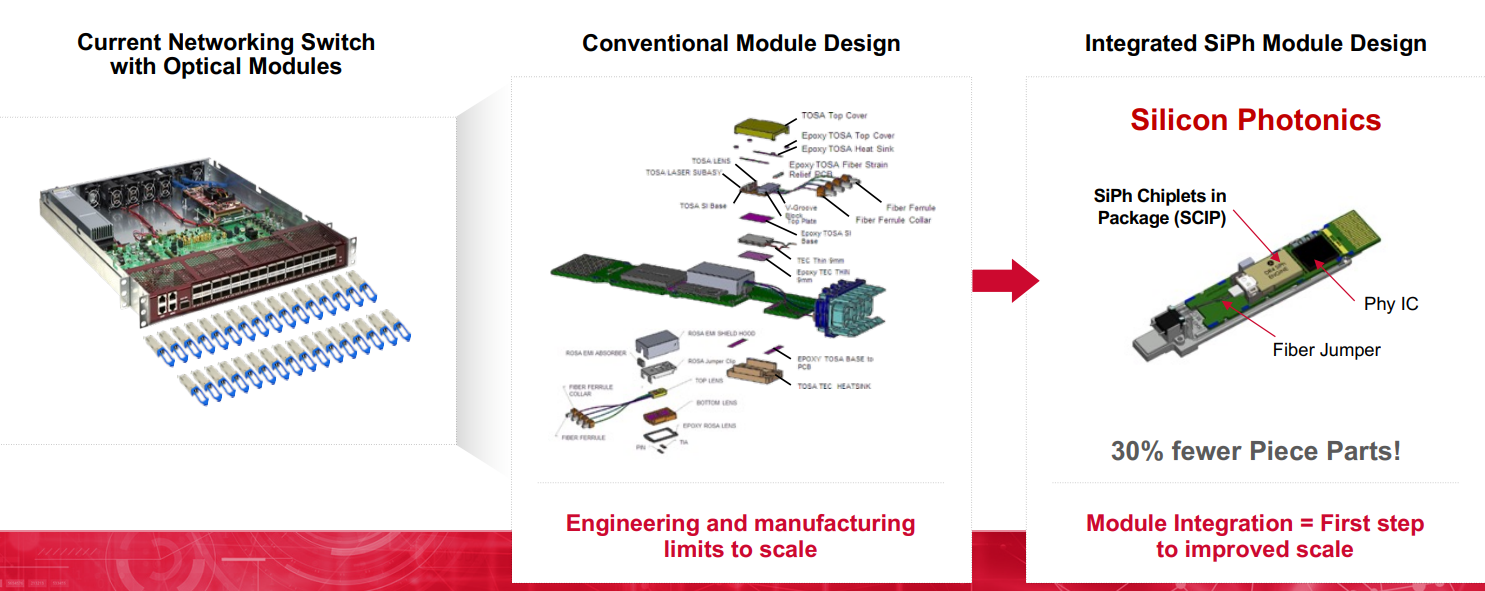
Broadcom was able to demonstrate significant power savings with its co-packaged optics, which the company said uses 30% fewer parts. The company took standard 800G pluggable modules and compared its co-packaged optics at the same spec. The pluggable module drew 14 watts of power, while Broadcom’s co-packaged optics drew less than half of that power at 5.5 watts.