Datanami
 EnterpriseAI
 HPCwire Japan
 QCwire
 HPC & AI Wall Street
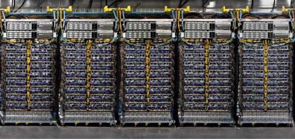
There are limits on the speed at which copper wires can move data between computers, and a transition to light speed will ultimately drive AI and high-performance computing forward. Every major chipmaker is in agreement that optical interconnects will be needed to reach zettascale computing in an energy-efficient way – an opinion shared last month by AMD’s CEO Lisa Su.
Google has experimented with and deployed optical interconnect between servers and chips in its datacenter. In an arXiv paper released last week, the company shared details about its implementation and the gains in performance and power efficiency.
Google talked about the TPU v4 supercomputer, which has 4,096 of the company’s Tensor Processing Units (TPUs). Google runs its AI applications on TPU chips, and that includes Bard, which is an early iteration of the company’s AI-infused search engine. The company has deployed dozens of TPU v4 supercomputers in Google Cloud.
Google’s paper on its supercomputing infrastructure comes after Microsoft made noise about its Azure supercomputer with Nvidia GPUs, which powers ChatGPT. By comparison, Google has been conservative in deploying AI in its web applications, but is now trying to catch up with Microsoft, which has deployed OpenAI’s GPT-4 large-language model in its Bing search engine.
Optical connections have been used for long-distance communications over telecom networks for decades, but now are considered ripe for use over shorter distances in datacenters. Companies such as Broadcom and Ayar Labs are creating products for optical interconnects.
Google’s TPU v4 supercomputer was deployed in 2020, and the paper was written as a retrospective piece that measures performance gains over the years.
The supercomputer is the “first with a circuit-switched optical interconnect,” Google researchers told HPCwire in an email. It had a total of 64 racks hosting 4,096 TPUs, plus 48 optical circuit switches connecting all racks across the system. Google calculated that the optical components account for under 5% of the system cost and under 2% of the power consumed by a system.
The TPU v4 chip outperforms TPU v3 chips by 2.1 times and improves the performance per watt by 2.7 times, Google researchers wrote. “The TPU v4 supercomputer is 4x larger at 4096 chips and thus ~10x faster overall, which along with OCS flexibility helps large language models,” the researchers said in the paper.
Google highlighted the flexibility of optics in deploying systems and adapting the topology on the fly depending on the application; the optical interconnect and its high bandwidth allowed each rack to be deployed independently, and each rack could be plugged in once production was completed.
“Incremental deployment greatly improved the time to production use and thus cost effectiveness of the TPU v4 supercomputers,” the researchers said.
It was quite a different story for the predecessor TPU v3 supercomputer, which had a total of 1,024 TPU chips. “TPU v3 systems were not usable until all 1,024 chips and all cables were installed and tested. Delivery delays for any component held up the entire supercomputer,” the researchers wrote.
Google described its optical circuit switching as a next-generation interconnect compared to Nvidia’s NVSwitch, which is based on electricals. The optical switches are ” fibers connected by mirrors, so any bandwidth running through a fiber can be switched between input and output fibers by the OCS across 4,096 chips today,” Google researchers said.
The interconnect will be scalable to more TPU cores and can establish multiple terabits per second links.
The research paper compared the TPU v4 chip to Nvidia’s A100 chip, which was also used in 2020 and made using the 7nm process. Nvidia’s recent Hopper H100 was not available in cloud until earlier this year, and Google left the option open to compare its next-generation TPU v5 to the H100.
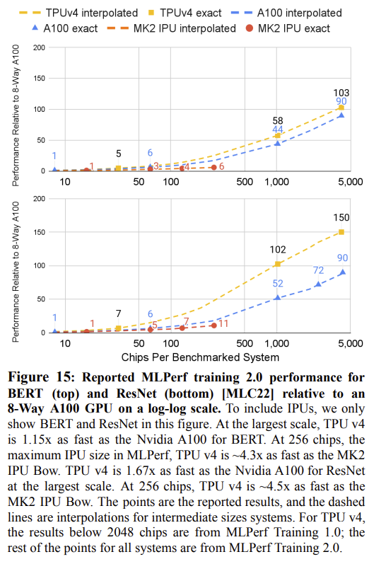
Google claimed its chip could outperform A100 and an AI chip from Graphcore, but the researchers also opine on AI benchmarks like MLPerf, which measures peak performance for training and inference. Google researchers claimed its TPU v4 chips made better and more relevant use of computing resources in real-world scenarios.
“The HPC community is familiar with the gap between Linpack performance and the performance delivered on real applications, which the ACM Gordon Bell Prize recognizes. The most recent winner achieved 5%-10% of the Linpack’s flops/second on several HPC supercomputers. As the paper mentions, peak and delivered AI performance are not necessarily correlated. We are proud that a large language model trained at on average 58% of peak hardware performance of TPU v4 over 50 days,” Google researchers said in response to a question from HPCwire.
The TPU v4 supercomputer includes SparseCores, an intermediary chip that is closer to high-bandwidth memory, where a lot of the AI crunching takes place. The concept of SparseCores supports an emerging computing architecture being researched by the likes of AMD, Intel, and Qualcomm, which relies on computing coming closer to data, and orchestration between data movement in and out of memory.
The paper dedicated many pages comparing the TPU v4 supercomputer to Nvidia’s A100 on performance and energy efficiency metrics. Still, Google typically optimizes its applications for processing on its TPUs, which doesn’t make it an apples-to-apples comparison.
Google uses the optical circuit switch for other applications, which it detailed in a paper last year, but this is the first time it has created a large-scale optical interconnect.