Datanami
 EnterpriseAI
 HPCwire Japan
 QCwire
 HPC & AI Wall Street
The $54.2 billion U.S. CHIPS and Science Act – which was signed into law last August – included $11 billion for research and development efforts to be led by the Department of Commerce (DOC). Under that umbrella: the National Semiconductor Technology Center (NSTC), which was characterized by the Senate Committee on Commerce, Science and Transportation as a “public-private partnership to conduct advanced semiconductor manufacturing R&D and prototyping; invest in new technologies; and expand workforce training and development opportunities.”
Over the ensuing months, the DOC has been working to define the NSTC, issuing a request for information (RFI) that elicited responses from stakeholders along the semiconductor supply chain and hosting dozens of workshops and listening sessions. In the wake of those efforts, the DOC promised a Q1 2023 white paper. Now, that white paper has arrived – only slightly behind schedule! – and clears up some big questions about what the NSTC will look like.
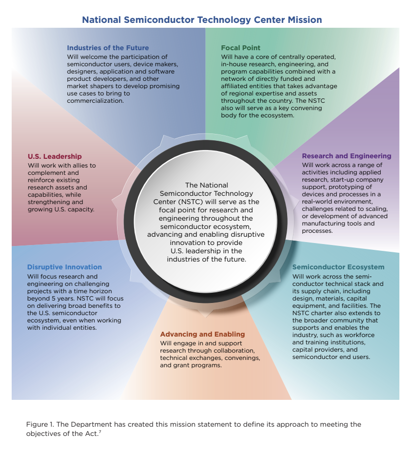
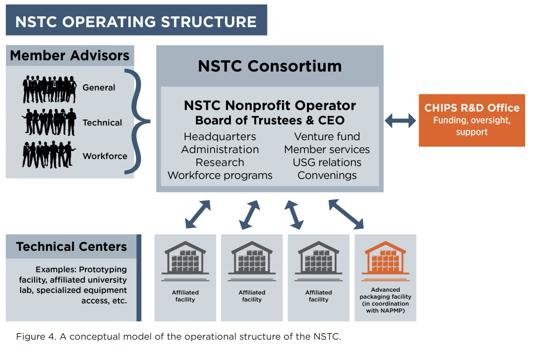
The NSTC, the authors explained, “will consist of a headquarters facility and an integrated network of NSTC-affiliated technical centers with locations geographically distributed to leverage existing capabilities.” The DOC envisions these centers as having capabilities for end-to-end fabrication for prototype and pilot runs, as well as capabilities for experimentation, testing and other related activities, with all of this functionality operating at a higher level than “what is feasible for universities, semiconductor startups, federal R&D facilities, and even some corporate R&D laboratories.”
The “exact makeup and number” of these facilities hasn’t been determined yet, but the paper notes that due to the “significant infrastructure costs” associated with new facilities, the DOC is exploring “new facilities, acquiring existing facilities, or collaborating between the NSTC and existing facilities with potential expansion and upgrade funding to meet the desired specifications.”
Included in the white paper is a list of “identified needs” for these centers from the aforementioned community input processes. These needs range from “baseline CMOS” process (22nm or below) to exploratory technology like bioelectronics.
The white paper also describes the “NSTC Design Enablement Gateway” to enable safe sharing of IP through a cloud-based gateway that would serve as a “focal point for semiconductor fabless R&D,” with resources including important tools like datasets and patents. (The community input includes suggestions like an “app store”-style environment.) The authors caution that such a gateway “is complex and many details are yet to be determined,” adding that the goal would be to reduce time and cost to market and to facilitate collaboration. Along similar lines, the NSTC will “establish and capitalize an investment fund to help emerging semiconductor companies advance their technologies toward commercialization.”
The paper also discusses workforce development programs that could be hosted by the NSTC centers or provided remotely. In a press release, the DOC said that the NSTC “will serve as a coordinating body and center of excellence to scale the technical workforce, including scientists, engineers, and technicians. The NSTC workforce programs will support expanding recruiting, training, and retraining for the semiconductor ecosystem, including reaching groups that are traditionally under-represented in the industry.”
The white paper also describes the NSTC’s membership and governance structures. The authors explain that the NSTC will be a membership-based organization with “different fees by scale of institution and by industry sector[.]” Membership is expected to be open to international companies and research organizations, provided they are not under the control or jurisdiction of “a foreign country of concern.”
Vis-a-vis governance, “the Department anticipates the creation of a new, purpose-built, independent, nonprofit entity with the requisite neutrality, expertise, leadership, and capacity to serve as the operator of the NSTC.” A graphic shows this operator having a board of trustees and CEO, as well as external advisors and the expected oversight from the CHIPS R&D Office.
“The NSTC will be an ambitious public-private consortium where government, industry, customers, suppliers, educational institutions, entrepreneurs, and investors will come together to innovate, connect, and solve problems,” said Secretary of Commerce Gina Raimondo. “Most importantly, the NSTC will ensure that the U.S. leads the way in the next generation of semiconductor technologies which can enable major new advances in areas that will advance our economic and national security. While the manufacturing incentives of the CHIPS Act will bring semiconductor manufacturing back to the U.S., a robust R&D ecosystem led by the NSTC will keep it here.”
The white paper includes much, much more detail and enumerates many more possibilities for the NSTC’s activities – so click this link if you’re interested in learning more.