 Datanami
 EnterpriseAI
 HPCwire Japan
 QCwire
 HPC & AI Wall Street
NEW YORK, July 14, 2020–Researchers at Columbia Engineering and Montana State University report today that they have found that placing sufficient strain in a 2D material–tungsten diselenide (WSe2)–creates localized states that can yield single-photon emitters. Using sophisticated optical microscopy techniques developed at Columbia over the past three years, the team was able to directly image these states for the first time, revealing that even at room temperature they are highly tunable and act as quantum dots, tightly confined pieces of semiconductors that emit light.
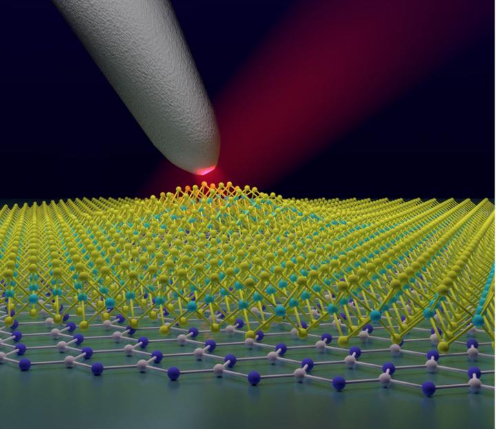
Image courtesy of Nicholas Borys/Montana State University
“Our discovery is very exciting, because it means we can now position a single-photon emitter wherever we want, and tune its properties, such as the color of the emitted photon, simply by bending or straining the material at a specific location,” says James Schuck, associate professor of mechanical engineering, who co-led the study published today by Nature Nanotechnology. “Knowing just where and how to tune the single-photon emitter is essential to creating quantum optical circuitry for use in quantum computers, or even in so-called ‘quantum’ simulators that mimic physical phenomena far too complex to model with today’s computers.”
Developing quantum technologies such as quantum computers and quantum sensors is a rapidly developing field of research as researchers figure out how to use the unique properties of quantum physics to create devices that can be much more efficient, faster, and more sensitive than existing technologies. For instance, quantum information–think encrypted messages–would be much more secure.
Light is made up of discrete packets of energy known as photons, and light-based quantum technologies rely on the creation and manipulation of individual photons. “For example, a typical green laser pointer emits over 1016 (10 quadrillion) photons every second with the mere push of a button,” notes Nicholas Borys, assistant professor of physics at Montana State University and co-PI of this new study. “But developing devices that can produce just a single controllable photon with a flip of a switch is extremely difficult.”
Researchers have known for five years that single-photon emitters exist in ultrathin 2D materials. Their discovery was greeted with much excitement because single-photon emitters in 2D materials can be more easily tuned, and more easily integrated into devices, than most other single-photon emitters. But no one understood the underlying material properties that lead to the single-photon emission in these 2D materials. “We knew that the single-photon emitters existed, but we didn’t know why,” says Schuck.
In 2019 a paper came out from the group of Frank Jahnke, a professor at the Institute for Theoretical Physics at the University of Bremen, Germany, that theorized how the strain in a bubble can lead to wrinkles and localized states for single-photon emission. Schuck, who focuses on sensing and engineering phenomena emerging from nanostructures and interfaces, was immediately interested in collaborating with Jahnke. He and Borys wanted to focus in on the tiny, nanoscale wrinkles that form in the shape of doughnuts around bubbles that exist in these ultrathin 2D layers. The bubbles, typically small pockets of fluid or gas that get trapped between two layers of 2D materials, create strain in the material and lead to the wrinkling.
Schuck’s group, and the field of 2D materials, faced a major challenge in studying the origins of these single-photon emitters: the nanoscale strained regions, which emit the light of interest, are much smaller–roughly 50,000 times smaller than the thickness of a human hair–than can be resolved with any conventional optical microscope.
“This makes it difficult to understand what specifically in the material results in the single-photon emission: is it just the high strain? Is it from defects hidden within the strained region?” says the study’s lead author Tom Darlington, who is a postdoc and former graduate researcher with Schuck. “You need light to observe these states, but their sizes are so small that they can’t be studied with standard microscopes.”
Working with other labs at the Columbia Nano Institute, the team drew upon their decades-long expertise in nanoscale research. They used sophisticated optical microscopy techniques, including their new microscopy capability, to look not just at the nano-bubbles, but even inside them. Their advanced “nano-optical” microscopy techniques–their “nanoscopes”–enabled them to image these materials with ~10 nm resolution, as compared to approximately 500 nm resolution achievable with a conventional optical microscope.
Many researchers have thought that defects are the source of single-photon emitters in 2D materials, since they usually are in 3D materials such as diamond. To rule out the role of defects and show that strain alone could be responsible for single-photon emitters in 2D materials, Schuck’s group studied the ultralow-defect materials developed by Jim Hone’s group at Columbia Engineering, part of the NSF-funded Materials Research Science and Engineering Center. They also leveraged new bilayer structures developed within the Programmable Quantum Materials Center (a DOE Energy Frontiers Research Center), which provided well-defined bubbles in a platform that was easily studied with Schuck’s optical “nanoscopes.”
“Atomic-scale defects are often attributed to localized sources of light emission in these materials,” says Jeffrey Neaton, a professor of physics at UC Berkeley and Associate Laboratory Director for Energy Sciences, Lawrence Berkeley National Laboratory, who was not involved in the study. “The emphasis in this work on the fact that strain alone, without the need for atomic-scale defects, potentially impact[s] applications ranging from low-power light-emitting diodes to quantum computers.”
Schuck, Borys, and their teams are now exploring just how strain can be used to precisely tailor the specific properties of these single-photon emitters, and to develop paths towards engineering addressable and tunable arrays of these emitters for future quantum technologies.
“Our results mean that fully tunable, room-temperature single-photon emitters are now within our grasp, paving the way for controllable–and practical–quantum photonic devices,” Schuck observes. “These devices can be the foundation for quantum technologies that will profoundly change computing, sensing, and information technology as we know it.”
About the Study
The study is titled “Imaging strain-localized excitons in nanoscale bubbles of monolayer WSe2 at room temperature.”
Authors are: Thomas P. Darlington 1, Christian Carmesin 2, Matthias Florian 2, Emanuil Yanev 3, Obafunso Ajayi 3, Jenny Ardelean 3, Daniel A. Rhodes 3, Augusto Ghiotto 4, Andrey Krayev 5, Kenji Watanabe 6, Takashi Taniguchi 6, Jeffrey W. Kysar 3, Abhay N. Pasupathy 4, James C. Hone 3, Frank Jahnke 2, Nicholas J. Borys 7, and P. James Schuck 3. 1 Department of Physics, UC Berkeley
2 Institute for Theoretical Physics, University of Bremen, Germany
3 Department of Mechanical Engineering, Columbia University
4 Department of Physics, Columbia University
5 Horiba Scientific, Novato, CA
6 National Institute for Materials Science, Tsukuba, Japan
7 Department of Physics, Montana State University
The study was supported primarily by the National Science Foundation, Division of Materials Research, under the Quantum Leap initiative (NSF-1838403).
The authors declare no competing interests.
LINKS:
Paper: https:/
DOI: 10.1038/s41565-020-0730-5
Columbia Engineering
Columbia Engineering, based in New York City, is one of the top engineering schools in the U.S. and one of the oldest in the nation. Also known as The Fu Foundation School of Engineering and Applied Science, the School expands knowledge and advances technology through the pioneering research of its more than 220 faculty, while educating undergraduate and graduate students in a collaborative environment to become leaders informed by a firm foundation in engineering. The School’s faculty are at the center of the University’s cross-disciplinary research, contributing to the Data Science Institute, Earth Institute, Zuckerman Mind Brain Behavior Institute, Precision Medicine Initiative, and the Columbia Nano Initiative. Guided by its strategic vision, “Columbia Engineering for Humanity,” the School aims to translate ideas into innovations that foster a sustainable, healthy, secure, connected, and creative humanity.
Source: Columbia University School of Engineering and Applied Science


