Datanami
 EnterpriseAI
 HPCwire Japan
 QCwire
 HPC & AI Wall Street
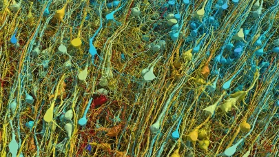
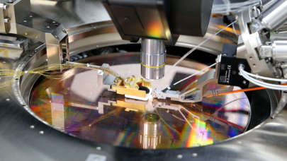
Quantum computing presents many challenges not least developing practical methods for fabricating qubits and the computers themselves. Last week researchers from MIT, Harvard, and Sandia National Laboratory reported a new method for creating tiny defects in diamonds and harnessing them for use in quantum systems. The work shows promise for scaling up quantum computer production.
Their paper, ‘Scalable focused ion beam creation of nearly lifetime-limited single quantum emitters in diamond nanostructures,’ published in Nature Communications, reports using focused ion beam technology to create interfaces between quantum memories and quantum networks. There is also an account on the MIT News web site, ‘Toward mass-producible quantum computers.’
 As the researchers note in their abstract, “The controlled creation of defect centre—nanocavity systems is one of the outstanding challenges for efficiently interfacing spin quantum memories with photons for photon-based entanglement operations in a quantum network. Here we demonstrate direct, maskless creation of atom-like single silicon vacancy (SiV) centres in diamond nanostructures via focused ion beam implantation with ~32nm lateral precision and 50nm positioning accuracy relative to a nanocavity.” (Process shown here with caption below, click to enlarge)
The lead researcher from MIT, Dirk Englund, associate professor of electrical engineering and computer science, is quoted in the MIT article saying, “The dream scenario in quantum information processing is to make an optical circuit to shuttle photonic qubits and then position a quantum memory wherever you need it. We’re almost there with this. These emitters are almost perfect.”
As explained in the MIT article, Diamond-defect qubits result from the combination of “vacancies,” which are locations in the diamond’s crystal lattice where there should be a carbon atom but there isn’t one, and “dopants,” which are atoms of materials other than carbon that have found their way into the lattice. Together, the dopant and the vacancy create a dopant-vacancy “center,” which has free electrons associated with it. The electrons’ magnetic orientation, or “spin,” which can be in superposition, constitutes the qubit.
A perennial problem in the design of quantum computers is how to read information out of qubits. Diamond defects present a simple solution, because they are natural light emitters. In fact, the light particles emitted by diamond defects can preserve the superposition of the qubits, so they could move quantum information between quantum computing devices.
Link to Nature Communications article: https://www.nature.com/articles/ncomms15376
Link to MIT News article: http://news.mit.edu/2017/toward-mass-producible-quantum-computers-0526
Figure Caption
Figure 1 | Targeted Si ion implantation into diamond and SiV defect properties. (a) Illustration of targeted ion implantation. Si ions are precisely positioned into diamond nanostructures via a FIB. The zoom-in shows a scanning electron micrograph of a L3 photonic crystal cavity patterned into a diamond thin film. Scale bar, 500 nm; Si is silicon. (b) Intensity distribution of the fundamental L3 cavity mode with three Si target positions: the three mode-maxima along the centre of the cavity are indicated by the dashed circle. The central mode peak is the global maximum. (c) Atomic structure of a SiV defect centre in diamond. Si represents an interstitial Si atom between a split vacancy along the o1114 lattice orientation and C the diamond lattice carbon atoms.
(d) Simplified energy-level diagram of the negatively charged SiV indicating the four main transitions A, B, C and D26. Do is the energy splitting of the two levels within the doublets.