Datanami
 EnterpriseAI
 HPCwire Japan
 QCwire
 HPC & AI Wall Street
GlobalFoundries (GF) and Ayar Labs, a startup focused on using light, instead of electricity, to transfer data between chips, today announced they’ve entered into a strategic partnership. The companies will develop and manufacture Ayar’s optical I/O technology using GF’s CMOS fabrication process to deliver an alternative to copper interconnects that offers 10 times higher bandwidth and up to five times lower power. As part of the agreement, GF has also invested an undisclosed amount in Ayar.
The partners say the collaboration will create unique and differentiated solutions for cloud servers, datacenters and HPC customers and will benefit from GF’s investment in 45nm CMOS technology.
Ayar Labs’ photonics devices will be manufactured on GF’s 45nm RF SOI (Radio Frequency Silicon on Insulator) process at its East Fishkill fab. GF says it expects to deliver prototype parts for Ayar Lab customers in 2018 and will be ready to support production ramp-up post successful qualification.

Although today’s announcement marks the start of a formal direct relationship between the companies, the researchers who formed Ayar Labs have using the fab’s technology to design silicon photonics components since 2009 but they did so via multi-project wafer runs, relying on aggregators who collect designs from university groups and startups that don’t have the resources to do full wafer runs.
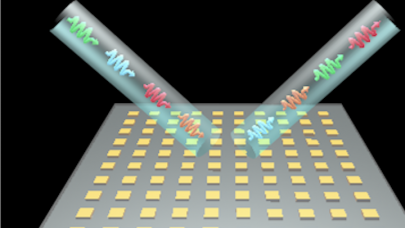
Ayar Labs was launched in 2016 by a group of researchers from MIT, UC Berkeley, and CU Boulder who were part of a 10-year research collaboration funded by DARPA. Their breakthrough was to put advanced electronics and optics on the same chip leading to the development of the first microprocessor chip to communicate using light, implemented via standard CMOS.
“They had a really interesting approach,” explained Alex Wright-Gladstein, CEO of Ayar Labs and one of its cofounders. “Instead of taking manufacturing methods from the optics industry which usually use materials like indium phosphide and different III-V materials, instead of using that set of techniques to make optics, they just said let’s try to use standard CMOS manufacturing, pure silicon, with no change to the standard CMOS process, and see if we can make optics work in that totally different framework and use optical I/O instead of electrical I/O, get rid of electrical I/O entirely, get rid of copper.
“While there’s been attention on longer distance optical communication, we’re doing shorter distances, trying to replace copper cables that are used inside datacenters and even the copper traces on printed circuit boards. We’re very excited about the partnership with GlobalFoundries, having their backing and validation, because it will help open up a new customer base to us and this partnership will help us qualify our products and get them into the market faster,” said Wright-Gladstein.

The problem that the technology is aiming to solve is well understood in HPC circles and in the semiconductor industry. Moore’s law has driven an exponential increase in the amount of computing power you can fit on a chip while the speed at which data moves in and out of chips has only made incremental gains. Over the past few decades, that has become a bottleneck so processors and servers can process huge amounts of data but spend a lot of time waiting to send and receive data.
The DARPA-backed research effort resulted in a chip with a bandwidth density of 300 gigabits per second per square millimeter, “about 10 to 50 times greater than packaged electrical-only microprocessors currently on the market.”
The technology is well described in the inventors’ December 2015 Nature paper, which HPCwire covered here. The first two authors, Chen Sun of UC Berkeley and Mark Wade of CU Boulder, are Ayar Labs full-time cofounders. The professors who co-authored the paper are part-time cofounders MIT’s Rajeev Ram, Vladimir Stojanovic at UC Berkeley, and Miloš Popovic from CU Boulder.
Improvements have been made in terms of data rates since the paper was published, Wright-Gladstein told HPCwire: “We’ve moved to standard wavelength ranges. We’re using O-band wavelengths rather than the non-standard 1,180nm that was described in that paper, but the fundamental architecture is still using that same approach so that micro-ring resonator based approach with dense wavelength division multiplexing (DWDM) at lots of wavelengths on a single fiber.”
Ayar’s first products will support 8 and 16 wavelengths of light on a single fiber and eventually they plan to go to 32.
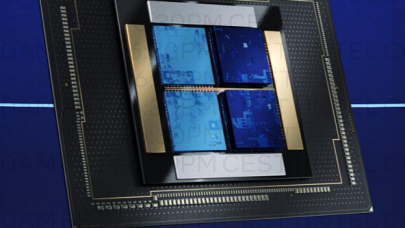
Ayar is implementing the technology in multi-chip modules, where you have chiplets in the same package with very short electrical links connecting them. “So it doesn’t really matter where the processor is getting made or what node it’s in,” said the CEO. “It can be a 7nm CMOS node with ultra short reach links coming out of it that just go to our very close chiplet that’s integrated in-package with that processor chip or similarly with a switch ASIC, for example. And because those electrical links are so short they are also very very low power so you end up enabling a full kit package with multiple chiplets in it that is lower power than if you were to have beefier electrical SerDes driving the signal a longer distance.”
Ayar is targeting two spaces initially: high-performance computing and the traditional datacenter. “Until now there’s always been a tradeoff between going to go to higher bandwidth in your network versus having low latencies, and we are not forcing system architects to have to make those tradeoffs,” said Wright-Gladstein, who points to the potential for speeding machine/deep learning training by enabling highly parallel models.
Ayar also believes its technology has a role to play in enabling disaggregated architectures. “Having bigger pools of processing power and memory makes it so you can be more flexible about how you allocate your jobs across your datacenter and reduce the amount of time that your resources are idling and not being used,” said the CEO.
In the big picture, Wright-Gladstein is bullish about the success of on-chip optical I/O in the datacenter, expecting that it will replace CMOS SerDes within the next 5-10 years, clarifying that “it’s just the I/O portion that I think will be replaced, the power is we’re still using CMOS for everything else.”
“It’s pretty clear that we’re at the end of CMOS electrical I/O and being able to scale electrical SerDes as we have in the past,” she continued. “25 gigabits per second per pin is where we are today and people are working on 50 gigabits per second per pin. There’s a cadence of doubling that bandwidth every few years but folks are starting to struggle with the idea of moving to 100 gigabits per second per pin electrical SerDes and it’s tough to imagine going beyond that so something else needs to come along and [Ayar] technology which offers a 10x improvement rather than the standard 2x is really going to be an enabler for that.”

While the Ayar CEO envisions light displacing electrical communications in the near future, over the longer term, she sees opportunities for silicon photonics beyond I/O, for example in quantum computing. She relates that teams looking to use optics for quantum computing face challenges with respect to manufacturability where it’s difficult to achieve the high consistency (low variation) that optical devices demand and high yield.
“At Ayar, we get to use this massive ecosystem of CMOS manufacturing, having GlobalFoundries, a standard CMOS fab, manufacturing our chips, something that is totally unique within optics,” she says. “Most optics manufacturing is much lower volume and much lower yield, but just the fact that billions of dollars have been poured into the CMOS manufacturing ecosystem means it’s a much more reliable manufacturing flow with much better controls. So in the longer term we want to make our platform available to a wide range of different applications for optics, such as quantum computing, LIDAR imaging for self-driving cars, and many healthcare applications.”
Anthony Yu, who leads the silicon photonics business within GF, told HPCwire that the company plans to move to its next-generation 45nm photonics process in 2019. That will be a follow on to the 90nm photonics process running currently in GF’s East Fishkill facility.
“That will be a process design entirely for photonics, entirely for things like optical tranceivers and we’ll be taking up Ayar Labs technology in the pure photonics process and bringing about even more performance for both Ayar Labs and our customers,” he said.
Of course, Ayar and GF aren’t the only companies pursuing the potential and promise of silicon photonics. Intel and IBM have demonstrated multiple breakthroughs already and hyperscalers have considerable motivation to develop their own technologies. Competition is sure to be fierce.